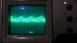
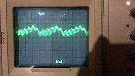
I've made the changes: added 100uF decoupling capacitors to the pcb main PS, resoldered 100pf cdom capacitors (50pF cdoms on another channel) after 220R of the bases of small VAS transistors (due to long distance) to the collectors of another VAS transistors. Here is the result. I remind that this is other channel with different bias schematic which is shown on pcb layout.
In the past I already tried to place cdoms this way, but observed worse results than at B-C of TO126 transistors.
Perhaps the problem in the input stage, maybe due to long leads of input transistors or pcb traces signal coupling?
In the past I already tried to place cdoms this way, but observed worse results than at B-C of TO126 transistors.
Perhaps the problem in the input stage, maybe due to long leads of input transistors or pcb traces signal coupling?
Attachments
Last edited:
I am afraid your variant layout without a plane layer between the routing layers will exhibit the same issue you are facing now.
You should familiarize with the concept of ground planes and high speed routing techniques.
Do you mean 3 or 4 layer pcb? Could you please advise where can I familiarize myself with the concept of ground planes and high speed routing techniques?
Thanks and Regards.
This is a classic reference for high speed stuff...
High Speed Digital Design: A Handbook of Black Magic: Howard Johnson, Martin Graham: 9780133957242: Amazon.com: Books
It's digital in its orientation, but gives enough of the background so you understand things in an analog context.
As to PCB's, they come in 1 layer, and then above that I only have ever seen even layer counts...so possible boards would be 1 layer, 2 layer, 4 layer, etc...that is to say - - no 3 layer boards.
Do you mean 3 or 4 layer pcb? Could you please advise where can I familiarize myself with the concept of ground planes and high speed routing techniques?
Thanks and Regards.
@AndriyOL,
sure, djoffe already offered an excellent source, he beat me to it

But I offer you another source. I have had the unique pleasure and opportunity to attend some of Dougs lectures and presentations.
I highly recommend this material to you, a truly eye-opening experience !
PCB Currents
You can easily do a two layer board with your design but effectively it will leave you with only one routing layer as the other layer is going to have to be a solid ground plane.
So in short no, I did not mean 3 or 4 layers.
You could however go with a 3 or 4 layer board. But why ?
A 3 layer board is going to cost you as much, perhaps more, that a 4 layer board. Boards are most cost effective if the layer count is an even number.
In case you feel you must use more layers, this is how I would go about.
L1.) routed signals
L2.) solid ground plane (no openings, cuts, interruption, slots or traces allowed)
L3.) routed signals
For power amps with higher power, lets say more than 50W, consider heavier copper cladding than just the standard 1oz copper on the outer layers. (yes this will cost more)
But before jumping in and redoing your board, look at the material otherwise you might repeat mistakes yet more costly.
@AndriyOL,
You can easily do a two layer board with your design but effectively it will leave you with only one routing layer as the other layer is going to have to be a solid ground plane.
Permit me to say it once again . You do NOT need a solid ground plane for a power amplifier.
I have never used one in any product. Waste of a layer.
Permit me to say it once again . You do NOT need a solid ground plane for a power amplifier.
I have never used one in any product. Waste of a layer.
Douglas,
with all utmost and due respect, I must say I am very very disappointed to learn that you feel that way.
It certainly has been demonstrated that having a ground plane in combination with star grounding gives very good results. From that aspect, I would not want to refer to that as a waste of a layer, rather the opposite.
However I would say that, putting new modern components on a double sided board without a solid ground plane is nothing but a great EMI mess in the making, in particular when it is done by a hobbyist, that is in my opinion a waste.
Why not utilize the second layer for a ground plane when by doing so one can sidestep all the issues that make one loose hair over it, e.g. spurious oscillation and instability besides the EMI issues ?
I have your books and find them very useful. In your book the reader could get the impression you feel a little derogatory towards a PCBdraftperson as you seem to credit him/her at best for his skill to use a complex CAD software. In today's PCB world the so called PCBdraftperson must understand a great deal of AC signal flow, something a circuit designer never seem to bother with, perhaps its to lowly. Let me remind you it is the finished layout that makes the designed circuit work to its full potential or not as seen by the grief AndriyOL is facing. I am certain industry professionals like Susy Webb, Rick Hartly and Douglas Brooks would agree.
In your book you give very general layout advise but you do not cover the discussed aspect of signal return currents very well with respect to PCB layout.
Again, with the utmost and due respect, I do believe you can gain some benefit from Douglas publication, if you choose to do so.
PCB currents introduction video
I would be more than delighted to find you revise your opinion on ground planes and devote a chapter on the subject of usefulness of ground planes, signal return path, loop area and signal integrity, if you choose to do so.
@AndriyOL
Some reading for you.
http://www.ultracad.com/articles/loop.pdf
http://www.ultracad.com/articles/slots.pdf
http://www.ultracad.com/articles/crossemianddifferentialz.pdf
Keep in mind these papers are written with reference to digital circuitry, however the concepts discussed are of analog nature and are applicable to audio amplifier design, even tho some designers may insist otherwise.
Quote:
Summary:
These examples illustrate that the occurrence of loop areas can be pretty subtle. They can occur in places and at times that we wouldn't intuitively expect.
So designers are well counseled to keep two things in mind during the design process:
(1) all signals have a return path, and
(2) you really ought to know where they are !
It sometimes is not apparent or recognized that there is a slot in an internal plane, especially to an engineer or technician who didn't design the board. After the prototypes are built, the engineer discovers that he has unwanted reflections on a trace, EMI radiation, and crosstalk problems. He checks the traces and verifies that the impedance control guidelines (trace thickness and spacing) have been met, the routing is seemingly good, and the crosstalk control guidelines (trace separations) are correct. The effects of slots are really subtle and difficult to recognize. It doesn't occur to the engineer that the problems are related to the planes rather than to the traces.
Some engineers spend an enormous amount of time and, unfortunately, never find the real problem in the board design.
Responsible designers don't do this to their associates!
Summary:
So any wire or trace carrying an AC signal radiates a changing electromagnetic field. This can be a bad thing when the field causes crosstalk in an adjacent wire or trace, but a good thing when it couples to its differential pair. It can be a bad thing when it couples (radiates) to a trace or an antenna further away (e.g. at an FCC compliance testing range),
but a good thing when we are electronically transmitting a radio or television signal. Our jobs as engineers and designers is to understand how to control these fields and how to minimize those we don’t want and how, perhaps, to maximize the ones we do want.
EndQuote
Last edited:
Good articles.
It seems to me that many very fine audio amplifiers have be made with single and two layer boards.
Multilayer boards were expensive and also slow to prototype.
These days we can get affordable 4 and 6 layer PCBs pretty quickly.
Having mostly worked in RF and high speed, I tend to default to thinking a ground plane is something we should take for granted.
Generally, having a good ground plane is a sign that your circuit won't be a nightmare when it goes for EMC approval.
But it's not always so.
I can recommend books by Tim Williams and Henry Ott.
I have no Earth GND in my wall socket (have to rebuilt a mains wiring in my house).
I have only just spotted this.
It sounds like a very dangerous situation.
Yes, life is dangerous. Our safety standards do not require this as obligatory on every socket, only on a main switch.
Does anybody know, how to make a holes in a plane ("zone" of app terminology) for components not connected to the plane in Sprint L?
Also, can the pcb layout be simulated for unwanted effects (emi, crosstalk, couplings, etc.) as the schematic?
Does anybody know, how to make a holes in a plane ("zone" of app terminology) for components not connected to the plane in Sprint L?
Also, can the pcb layout be simulated for unwanted effects (emi, crosstalk, couplings, etc.) as the schematic?
Last edited:
Don't know about sprint but I would have though all PCB packages allow you to create a basic power plane even if it is only an old fashioned negative plane.
Sprint-Layout
Automatic Ground-Plane feature...
http://sp-hm.pl/attachment.php?aid=187
Page 31.
EMC advisers, signal and power integrity simulation is available on higher end PCB design packages at a cost.
For high speed simulation you model the probes you will be using fro measurements so you can switch them in and out of the signals being simulated, so you get a view of the signal as is and an image of the wave with the scope loading added.
For fun...
http://www.elmac.co.uk/Lord_of_the_board.pdf
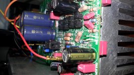
I can't help but notice from the pics of PCB that board look very contaminated with bits of solder. The soldering look rough with usually means it cold.
You need to clean away all the contamination and heat you joint until the solder flows smoothly.
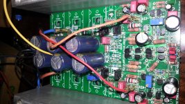
It was drilled into me many years ago by electrical engineers to not route trace underneath components particularly in power circuits. Avoid it at all costs.
Additionally It a good idea to leave more space between components. This from EEs who designed high speed data collection and transmission systems for particle accelerators (cyclotrons).
Sometime the shortest routing is not the best approach if it leads to component crowding. If you look at Douglas Self's successful designs you will notice ample space between components.
I repaired audio power amps for 15 years. The one's that failed the most where the high density layouts.
Maybe I missed the results but did you do the grounded enclosure test I suggested?
You need to clean away all the contamination and heat you joint until the solder flows smoothly.
It was drilled into me many years ago by electrical engineers to not route trace underneath components particularly in power circuits. Avoid it at all costs.
Additionally It a good idea to leave more space between components. This from EEs who designed high speed data collection and transmission systems for particle accelerators (cyclotrons).
Sometime the shortest routing is not the best approach if it leads to component crowding. If you look at Douglas Self's successful designs you will notice ample space between components.
I repaired audio power amps for 15 years. The one's that failed the most where the high density layouts.
Maybe I missed the results but did you do the grounded enclosure test I suggested?
It was drilled into me many years ago by electrical engineers to not route trace underneath components particularly in power circuits. Avoid it at all costs.
But why?
- Status
- This old topic is closed. If you want to reopen this topic, contact a moderator using the "Report Post" button.
- Home
- Amplifiers
- Solid State
- One of the Top Solid-State CFA amp design