Damir, this one is your latest schematic?I have CFA thread with triple BJT OPS. I never built that amp but some others did.
http://www.diyaudio.com/forums/solid-state/253039-unique-cfa-120-230w-amp-24.html#post4599024
Does anyone know of a simple add-on to make the standard Lin topology (or CFA) output transistors stay slightly on (about 30mA is enough) to keep the FT high? It might help the PM.
I guess it will be interesting to check out. Perhaps Class AC could be a solution from post 11.
Darlington or Sziklai (compound) pair output stages?
Ian, are Q6 and Q7 required in your schematic or can be omitted? There are no such transistors in Damir's IPS. Perhaps they could introduce additional noise figure.
Last edited:
Ian, are Q6 and Q7 required in your schematic or can be omitted? There are no such transistors in Damir's IPS. Perhaps they could introduce additional noise figure.
They are diodes (aka transdiodes). They are needed for thermal balancing and averaging out the offset voltage differences between PNP and NPN's. They are part of the Rush package deal. As diodes they don't contribute much noise but Rush pairs do reduce the gain so indirectly you get less gain and more noise due to less feedback. I don't think the noise level will be an issue.
I tried a capacitor across the 15k feedback resistor. With 2p2 it improves the phase margin to 59 degrees (was 23deg) which removes the peaking in the AC closed loop plot and a slight overshoot in the squarewave plot. A 2p7 removes the squarewave overshoot. This is SE without the input filter.

The squarewave sim circuit is attached. It includes the Tian probe to measure the PM accurately with this 2p2 capacitor (it is disabled in the attached circuit).
BTW I disconnected the cross-coupling capacitor C20+R42; with it there is some HF ringing in the squarewave in the higher voltage range, but stops when they are disconnected.

I have found a capacitor across the feedback resistor usually causes oscillation even though a simulation shows it works well. So I wouldn't feel too satisfied that the PM issue is fixed that easily. It is the first thing to try and if it works as well as it simulates then it's easy, and if not you need a plan B from a few more options that we have yet to try.
Attachments
Damir, this one is your latest schematic?
Yes, but I never built it and could be change in the process.
more options for compensation
Attached is the amp without the buffer since you said recently that you can make the buffer on a separate board.
The attached circuit also includes 100nH inductors in series with the emitter resistors and 50nH in series with the power transistor bases.
These inductor's stabilize the amplifier and they make all the difference to the simulation GM and PM (try different values for inductor's using the probed simulation). This seems to run contrary to the text book method of using low inductance emitter resistors, but this simulation shows that a small amount of emitter resistor inductance can help HF stability in the 20-50MHz region. (It may be triple power stages benefit more than doublets -- but I haven't checked if adding emitter inductance to doublets helps them as well.)
The gain margin is now 6dB and 36 degrees using the same Miller capacitors (two 39pF) as previous versions; Increasing the Miller capacitor can give more PM but at the expense of THD. The feedback at 1kHz is as before with THD ~2ppm at 1kHz and 15Vpk. Slew rate is 300V/us with no input filter capacitor and 150V/us with 220pF.
Notice also the Miller capacitors have been rearranged with a jumper. This is so they can now feed into a common node then on to both VAS bases. This jumper is normally closed. It can be opened to compare the difference without the linking of bases for simulation demonstration purposes (it's not on the final PCB).
With the link open it is possible to see slew rate failure with a fast rise 2V input. It seem to be because one of the Miller capacitors can charges faster than the other causing one side to swings by say -30V and the other side collapses close to zero volts (and not get to +30V). But with the jumper closed both VAS sides keet in sync. Also, the two Miller capacitors can be merged into one (68pF) in the final circuit, making changes easier.
These compensation changes could be called enhanced Miller compensation -- it is still -20dB decade roll-off but with various 'tweaks' to improve the PM near 180 degrees. BTW The 2p2 capacitor across the feedback resistor is fairly sensitive, so it would need to be a 10pF trimmer with a 10pF series capacitor.
I haven't tried two pole compensation or output inclusive compensation. If you are happy with the latest tweaks then you could proceed to add then to your PCB and run the amp again to see if they solve the oscillation problems.
Cheers
Hi AndriyOL,... a few more options that we have yet to try.
Attached is the amp without the buffer since you said recently that you can make the buffer on a separate board.
The attached circuit also includes 100nH inductors in series with the emitter resistors and 50nH in series with the power transistor bases.
These inductor's stabilize the amplifier and they make all the difference to the simulation GM and PM (try different values for inductor's using the probed simulation). This seems to run contrary to the text book method of using low inductance emitter resistors, but this simulation shows that a small amount of emitter resistor inductance can help HF stability in the 20-50MHz region. (It may be triple power stages benefit more than doublets -- but I haven't checked if adding emitter inductance to doublets helps them as well.)
The gain margin is now 6dB and 36 degrees using the same Miller capacitors (two 39pF) as previous versions; Increasing the Miller capacitor can give more PM but at the expense of THD. The feedback at 1kHz is as before with THD ~2ppm at 1kHz and 15Vpk. Slew rate is 300V/us with no input filter capacitor and 150V/us with 220pF.
Notice also the Miller capacitors have been rearranged with a jumper. This is so they can now feed into a common node then on to both VAS bases. This jumper is normally closed. It can be opened to compare the difference without the linking of bases for simulation demonstration purposes (it's not on the final PCB).
With the link open it is possible to see slew rate failure with a fast rise 2V input. It seem to be because one of the Miller capacitors can charges faster than the other causing one side to swings by say -30V and the other side collapses close to zero volts (and not get to +30V). But with the jumper closed both VAS sides keet in sync. Also, the two Miller capacitors can be merged into one (68pF) in the final circuit, making changes easier.
These compensation changes could be called enhanced Miller compensation -- it is still -20dB decade roll-off but with various 'tweaks' to improve the PM near 180 degrees. BTW The 2p2 capacitor across the feedback resistor is fairly sensitive, so it would need to be a 10pF trimmer with a 10pF series capacitor.
I haven't tried two pole compensation or output inclusive compensation. If you are happy with the latest tweaks then you could proceed to add then to your PCB and run the amp again to see if they solve the oscillation problems.
Cheers
Attachments
In triple Darlington output stages, the most important thing is to decouple the drivers and predrivers with RCs on the rails, because the output transistors generate enough RF rail fluctuations to cause positive feedback to the drivers.
I wouldn't be too dependent on the emitter inductors. Real life has a tendency to behave a lot different in that region than what the simulator predicts. I suspect some transistors may have more phase shift at RF than is in the models (which is more complex than Ft). It's hard to model this correctly because manufacturers rarely give s-parameters for audio transistors. If only I had a network analyzer...
I wouldn't be too dependent on the emitter inductors. Real life has a tendency to behave a lot different in that region than what the simulator predicts. I suspect some transistors may have more phase shift at RF than is in the models (which is more complex than Ft). It's hard to model this correctly because manufacturers rarely give s-parameters for audio transistors. If only I had a network analyzer...
Attached is the amp without the buffer since you said recently that you can make the buffer on a separate board.
Aren't those gain and phase margins too low, below the stability recommended values?
Hi carlmart,...Perhaps Ian can add the probes to your asc files, and comment on the results.
On the simulations he uploaded I got low margins. Are they satisfactory?
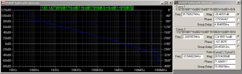
AndriyOL's sim4 circuit gives 29dB, 72 deg. See attached.
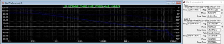
My earlier circuit in Post 564 (sim4e) giving 6dB and 36 degrees, and yes, it has no margin of safety for when building it. It needs double those figures as a safety margin to cover any modelling omissions. The post was following a series where I was trying different ways to get a bit more from the simple Miller compensation which was fixed at 39pF for a like-to-like comparison with the earlier circuits.
@All
Post 564 also raised the interesting question about the inclusion of inductors in the power transistors bases and emitters and keantoken commented on that Post 565.
The lack of model accuracy over the 10-50MHz region of our models places a degree of uncertainty on the GM and PM values we obtain using the Tian probe for instance. So we can't rely on our actual GM and PM values too much from simulations -- we need to test our built amps with a squarewave or whatever to see how close our sims actually were.
Where our GM and PM sims can help us is to compare different compensation methods in a relative way to get an idea of which type of compensation is best suited to our needs and aims.
Attachments
Yes, and if you follow it... goes all the way out to the ac power lines, modulating them as well.
I have network analyzers..... whatchew you need?
THx-RNMarsh
@ what frequencies are these rf gremlins, (trouble makers)?
Hi carlmart,
AndriyOL's sim4 circuit gives 29dB, 72 deg. See attached.
@All
Post 564 also raised the interesting question about the inclusion of inductors in the power transistors bases and emitters and keantoken commented on that Post 565.
The lack of model accuracy over the 10-50MHz region of our models places a degree of uncertainty on the GM and PM values we obtain using the Tian probe for instance. So we can't rely on our actual GM and PM values too much from simulations -- we need to test our built amps with a squarewave or whatever to see how close our sims actually were.
Where our GM and PM sims can help us is to compare different compensation methods in a relative way to get an idea of which type of compensation is best suited to our needs and aims.
If you check out some Harmon-Kardon service manuals e.g. HK870 it can be seen the driver stage is a complementary feedback pair arrangement and this stage feeds paired emitter followers via 10R resistors with Ferrite Beads shown as parallel inductors.
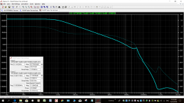
Ideally there should be no peaking. There is some at the top end of the frequency range on the plot. That could be a worry if there is stray capacitance or inductance in the wrong place with an actual build.
I imagine the Harman-Kardon approach is to damp some resonance giving rise to an unwelcome peak.
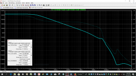
Nice to see you back Mjona. I think there is no such peaking now.
This is just a temporary visit as your support seems to have gone quiet for the moment.
You need a minimum phase margin of 45 degrees with a gain margin of 12dB for a circuit to be stable your latest circuit comes in at 29 degrees and 11dB which can be improved.
While that might get you inside the door albeit you should increase the margins to allow for component and simulation tolerances.
The first attachment shows what you have now - the simulation I am attaching shows changes to the lag compensation capacitors C3 and C5 and the disabling C21 which is responsible for the peak issue.
To use the simulation file you need to copy the following expression and paste it in the title of the .raw file where it says vout.
Right click on this and a drop-down box will open - in this you then delete vout and paste in the expression -1/(1-1/(2*(I(Vi)@1*V(x)@2-V(x)@1*I(Vi)@2)+V(x)@1+I(Vi)@2))
After that open the cursor options so you can place one firstly at 0 dB and the second where the angle shows at -180. You can drag these cursors close as you can to these points and use the side-ways movement arrow buttons - beside your number key pad to the right on your keyboard - to make fine adjustments either way.
Attachments
This one should be better.
I suggest to replace Vbe multipl. transistors with SOT23 or smaller devices and glue them to collector lead of OP devices for better bias tracking. Which transistors will fit the best in this case? As I know it should be high hFe.
Maximum power dissipation for VAS transistors and predrivers is not more than 1W, thus no any additional heatsinks required.
Attachments
You could use a string of diodes with a series resistance to drop the correct bias voltage. With rectifier types you could drill holes in the heat sink for the output devices and glue them in place.
The present bias system involves transistor emitter diode junctions and separate small signal diode types in series with resistors. There is nothing finicky about a string of diodes and these will be more reliable.
The present bias system involves transistor emitter diode junctions and separate small signal diode types in series with resistors. There is nothing finicky about a string of diodes and these will be more reliable.
While a phase margin of 45 degrees is a minimum requirement for stability according to one internet source the optimum for transient response is a margin of 60 degrees.
There is no guarantee that a simulated margin of 45 degrees is going to result in reality due to layouts, component tolerances etc so I have revised the simulation in my last post accordingly.
R17 and R18 values may need adjustment in that scenario as these have been used to flatten a peak into a temporary plateau.
Attachments
Actualy I already made one channel with bias setting by 1N4004 diode string wrapped by collector lead of OP transistors. As I can see this channel is more prone to ocsillation than with Vbe multiplier
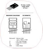
Thermaltrak transistors include diodes. The attached image shows the lead outs for emitter and collector.
This is by design to make it easy for the input leads to run closely as possible in order to minimise radiated magnetic fields into conductors in the proximity due to current changes due to OP switching.
The tracking diode leads run in parallel for similar reasons and if there is any length in the path of the wiring the solution is to twist these together.
Attachments
- Status
- This old topic is closed. If you want to reopen this topic, contact a moderator using the "Report Post" button.
- Home
- Amplifiers
- Solid State
- One of the Top Solid-State CFA amp design