Hi Damir,
I haven't changed the compensation since mjona's CFA version (before adding the Rush mods). The Rush mods add extra phase shift due to the extra transistor in the feedback path (Q8,Q9 sim4b). I was surprised it did not oscillate when I went from CFA to VFA by adding the Rush mods, which seems to suggest there is not a big difference between CFA and VFA modes, at least for this amplifier. By all means have a go at trying to improve the GM an PM, then compare it to your OITPC. I'd like to see how you will do it for this amp.
Re gain difference equalizing. As I mentioned a few posts back I have no working experience with balanced amps and I will take your word that the 2nd buffer is not necessary. When you call one input the "cold end" does that mean that input (inverting) is connected to ground somewhere? I assumed a balanced system was fully floating and both inputs are "live" (although one can be grounded if wanted yet without introducing hum pickup). Can you give a link or reference to what setup is commonly used for balanced amps?
Hi Jean,
I don't have practical experience with balanced input, just theoretical what i have read or learned.
Hot means non inverting and cold is inverting. I think that is standard to have the ground not floating, but don't take my word for it.
I don't have specific links, try search in this forum.
If this amp to has good enough PM as 60 degree or more the compensation caps should be increased over 100pF and distortion at 20 kHz rises ten times.
In my opinion the same instability problem was with non balanced version.
I don't think that OITPC could be easily used here, it needs more changes in VAS and OPS, I tried simple insertion but with not good result.
BR Damir
By the way this is not any more Rush cascode.
Last edited:
Thanks Damir,...I don't have specific links, try search in this forum.
I found this helpful XLR balanced cable using 3 core cable with a link to Jim Brown's articles Audio Systems Group, Inc. Publications scroll down to the Pin 1 problem
“Neil Muncy called our attention to the Pin 1 problem (the improper termination of the shield of audio wiring to the circuit board rather than to the shielding enclosure) in his classic 1994 paper, reprinted in the June 1995 Journal of the AES. When he wrote his paper, most commercially available audio gear had pin 1 problems. It was, indeed, difficult to find equipment without it -- even the most prestigeous consoles had serious pin 1 problems! Over the next decade, the better manufacturers redesigned their products to correct their mistake, but sadly, many have not done so.”
That adds an extra twist!
 A lot to read and digest let alone do. I'd prefer to leave this one to the experts.
 Someone mentioned the "bi-phase" form of balanced outputs, where two opamps feed opposite phase with respect to ground, these cannot have one of the two lines grounded. Only true (floating) sending ends allow one of the two signal lines to be connected to common as a "cold side".
My impression is the balanced approach is not necessary for DIY to get hum free systems. Maybe balanced is easier to get hum free as plug and play (not plug and pray) for commercial systems. As mentioned in post 521 in my experience lifting the mains earth with diodes (bridges) on all except one unit remains safe and is just as effective in complicated systems; but it may not be acceptable for commercial systems due to differing countries laws for ground breaking bridges (is there a Standard for diode ground breaking of equipment?)
What do you mean. Please elaborate.By the way this is not any more Rush cascode.
Nice work Ian. What scares me is transistors count - 32pcs TO-92 devices. To use as SE CFA we need to ground cold input?
Perhaps it will be wise to make a separate add-on ballanced input modules, if it's going to be a final approach.
Not at all balanced system is not necessary for high-end DIY. They can be used with DACs directly without bal to se converters. There is only I/V conversion will be required if not used in voltage out mode.
Last edited:
Hi Damir,Hi Ian...
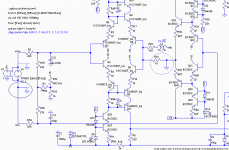
Could you show the Rush cascode(or pairs) in your post #539 schematic? I don't see it.
BR Damir
What about Q4+Q9 (likewise Q5+Q8)?
Cheers IanHegglun
Andriyol, good to hear from you.Nice work Ian. What scares me is transistors count - 32pcs TO-92 devices.
Damir said one buffer (noninverting) can go -- 8 less TO-92's. Using Rush pairs has increased the SE input stage count by 6.
A separate module for the inverting input would give the choice of SE or balanced. You can compare both, then decide before finalising a PCB.Perhaps it will be wise to make a separate add-on ballanced input modules, if it's going to be a final approach.
Yes, SE demands the cold input is to ground.To use as SE CFA we need to ground cold input?
BTW the SE cold input 'ground' is usually lifted from the power amp ground using a 10 ohm 1W resistor to stop hum loops between the sending units power ground and the amp. This resistor was on the very early circuits (here on LC's) but it has been removed for now and will be re-added for SE use. It connects to the inverting input's SE grounding resistor (R16 1k sim4b).
Re GM and PM. Damir found the present compensation give a 20 deg PM and changing the compensation to 100pF gave 60 deg but with 10 times THD at 20kHz. I assume you want to get the THD down to the 1ppm marks so 100pF compensation is not an option for you. Right? You cant rely on simulations to establish the compensation capacitor, you can only get ball park values to start with.
As for the Rush input stage adding more phase (reducing the PM) I did a simulation and compared it with mjona's Post 426 circuit. His PM was 16 deg or about the same as Damir's for the Rush version with the same 39 pF compensation and a 1nF load. The Rush version has about 6dB lower gain due to pairs having two b-e junctions in series which doubles THD at 20kHz (all other things staying the same).
I am happy with the Rush input stage as in Post 539 (sim4b) since it provides high input resistance for the noninverting input and a medium input resistance for the inverting input. Note the input asymmetry -- so you could get away with calling it a CFA topology
. Just to explain further, my earlier versions (Post 516 sim2b) had the same medium input resistances for the inputs and that's why I said it was VFA. I slipped in this change into sim4b without mentioning it.Hi AndriyOL,We can use RC or C compensation at VAS out instead of high Cdom. Perhaps in such a way the amp will show better THD. Like this.
It doesn't seem to help GM and PM.
BTW your circuit needs ".options maxstep=0.48831106u;1kHz"
and at least 3 cycles for a low noise floor, eg ".trans 3ms"
The attached circuit has the first buffer removed.
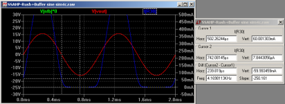
The AC plot shows how to measure GM and PM (this method is approximate only).
Disable the input filter (C13,C22 zero) and short cold side V3 to common for SE.

Move Cursor 1 to read -180 deg.
Move cursor 2 to 23.5dB.
Read the GM in dB and PM in deg.
Tip: It is helpful to read and write down the gain at 1kHz to compare if compensation is changed; then subtract 23.5dB (for 15k and 1k gain setting) to get net feedback dB (here 76dB). It shows how the THD at 1kHz will change with compensation changes (it's quicker than doing a .trans run to get the new THD).
Cheers
Attachments
Darlington OPS -- better PM?
Hi AndriyOL,
There should be better compensation methods to get low THD at say 20kHz. I'd prefer to stay with the simple Miller method for now until other methods are exhausted.
The attached circuit uses the standard triple Darlington with Laconthi 'T' resistors. I have reduced the base and emitter resistors to earlier values and biased for a higher current of 300mA to suit these resistors for minimum crossover distortion. A Darlington is known to be more stable at HF and with temperature changes than the other CFP. I also reduced the input stage current to 1.3mA to give more open loop gain.
The net open loop gain increase is about 6dB to 126dB. Then changing the compensation to 27pF to return to the same feedback at 1kHz as in earlier sims. The GM and PM are now 8dB and 25 deg, about the same as before (9dB and 22deg).
The THD at 1kHz with the buffer and inverting input shorted is the same 1ppm, or 0.08ppm without the inverting buffer. Notice most of the distortion at 1kHz is from the buffer which is outside the feedback loop.
The THD at 20kHz with the buffer and inverting input shorted is the same 2ppm, or 1.3ppm without the inverting buffer. At 20kHz most of the distortion is from the amp and not the buffer.
Overall, not much to be gained for GM and PM using this Darlington output stage over the previous CFP. I'd stay with the CFP unless you get HF oscillation problems when you make it (again).
Cheers
Attachments
I have CFA thread with triple BJT OPS. I never built that amp but some others did.
www.diyaudio.com/forums/solid-state/253039-unique-cfa-120-230w-amp-21.html#post4499907
Be careful with the triple, it needs some internal compensation otherwise it oscillate. I used 220pF between base and collector of the drivers, but better solution to use 47pF between base and collector of the predrivers.
Tip: It is helpful to read and write down the gain at 1kHz to compare if compensation is changed; then subtract 23.5dB (for 15k and 1k gain setting) to get net feedback dB (here 76dB). It shows how the THD at 1kHz will change with compensation changes (it's quicker than doing a .trans run to get the new THD).
Hi Ian,
What do you mean by 'subtract 23.5dB (for 15k and 1k gain setting) to get net feedback dB (here 76dB)'?
Why there is so much gain difference, and input impedance I guess, at hot and cold inputs: 1V vs 10mV input signals amplitude? Does it correct operation?
Do we really need L1 and L2 in the circuit? Are there a ways to further decrease components count?
What is output impedance (not at nfb node) of the amplifier now? Sorry, don't know how to measure it.
What's need to be removed (shorted to common) to use as SE, except cold input?
As I read before, there is other better in THD than Miller shunt method of compensation.
I think 300mA is too much bias, almost nobody will use such a big heatsinks required. In Roender's FC100 amp there is the same RE but 150-180mA bias set for minimum crossover distortion.
CFP is know to be more linear than Darlington output stage. I made it before and got HF oscillation without proper compensation and very low phase margin, as I've been advised. Now we can sim it before make it.
Last edited:
When you do an AC run you usually set the AC source to 1 volt. This gives 0dB on the magnitude axis. The amplifier has feedback attenuation of 15k and 1k so you subtract 20*log(15) or 23.5dB from the gain read at 1kHz to get the net gain that is available for feedback. This is the amount of gain that is available to reduces the distortion of the amp (which is mainly generated by the output stage), in this case the open loop distortion is reduced by 76dB at 1kHz with 39pF compensation.Hi Ian,
What do you mean by 'subtract 23.5dB (for 15k and 1k gain setting) to get net feedback dB (here 76dB)'?
Now, if you increase the compensation capacitor, or use your shunt compensation, or use any other type of compensation, then you can immediately get an estimate of what the new distortion will be at 1kHz without needing to go back to a .trans run to get the THD at 1kHz. EG 6dB less feedback means twice the THD. So you can save time this way.
You should find that when you increase the Miller compensation capacitors you will get better phase margin but higher distortion. You trade-off PM for THD. So the only way around this effect is to use a better type of compensation.
TPC. Two Pole Compensation can give better PM without raising distortion; it works by raising the slope of the roll-off before you get to 0dB net feedback, that's where the gain falls to 23.5dB for this amp. When you backup to 1kHz you can have a higher gain because the slope is higher. Ed Cherry used a similar approach and called it NDFL Nested Differentiating Feedback Loops).
OIC. Output Inclusive Compensation can utilize some of the feedback that is otherwise taken by Miller feedback and use it to reduce the output stage distortion. You can indirectly get more PM for the same feedback factor at 1kHz.
Damir said in Post 542 that his type of OIC+TPC for some reason did not seem to help this amp's PM (sim 4b I think).
Another way to improve the PM without trading THD at 1kHz is use a type of compensation that takes some of the gain below 1kHz (we have ~20dB available) and uses it to boost the gain just before 0dB net feedback. I think this is called "phase advance" compensation. EG Damir's capacitor across the VAS emitter degeneration, or a capacitor across the feedback resistor, or a capacitor from the VAS output to the input, called Miller Input Compensation (MIC).
I read in Bob Cordell's 1st Ed p91 "power amplifiers should have a gain margin of at least 6dB ... and a phase margin of at least 45 degrees". His Figure 4.10 shows a PM of 45 deg gives 3dB of peaking and 40% overshoot with a squarewave.
To get 0dB peaking the PM needs to be 58 degrees. So 60 degrees would be the ideal PM to aim for with a typical 500pF speaker cable. And the gain margin should be no less than 6dB.
Last edited:
The gain difference at the "hot" and "cold" inputs is normal. A similar query to previous. It is due to the action of feedback to the inverting input. It's basic to OPAMP's, these may help Opamp-1 Opamp-2 Opamp-8. With feedback the inverting input of the opamp becomes a "virtual earth" and has a low impedance. This means the new inverting input is taken before the input resistor and not the opamps inverting input. The new inverting input is now the "cold input".Hi Ian...
Why there is so much gain difference, and input impedance I guess, at hot and cold inputs: 1V vs 10mV input signals amplitude? Does it correct operation?
Do we really need L1 and L2 in the circuit? Are there a ways to further decrease components count?
For more details see Walt Jung's book here. It explains CFA's and p126 Fig.1-16 shows an early tube CFA.
Re L1 and L2. L1 is the output inductor. This has been covered previously. It is necessary to stop this amplifier oscillating when driving capacitive loads in the range of 2nF to 2uF. Commercial amps have to use it in case someone drives loads in this range (even then some commercial amps have 'smoked' when driving ESL's). DIY amps can often get away without L1 because the normal speaker cable load capacitance doesn't cause it to oscillate. You could include L1 and short it out with a wire bridge if you are comfortable enough to not use it at home. But if you drive ESL's or loan it out then be sure to break the shorting link.
L2 is not part of the amplifier
-- it is a clever trick that Bob Cordell has taught us -- it's to measure the open loop gain and phase of the amp while still preserving the DC operating point. It is there as a simulation aid. When you do an AC run you set L2 to say 1G Henry so the LF roll-off is below 1Hz and doesn't appear on the AC sweep from 1Hz up. When you do a .trans run you set L2 to 1n (Henry), so it is effectively a short giving us closed loop operation.AC runs are done open loop so we can view the GM and PM. One probe at -180 degrees requires a net gain of less than 1 or less than 0dB otherwise oscillation can occur, which usually destroys you amp in seconds. If the gain is slightly below 0dB then you get ringing; this indicates you are dangerously close to oscillation, hence the need to get closer to critical damping where ringing doesn't occur with a squarewave. PM is a better indicator of ringing and as mentioned earlier we should aim for about 60 degrees ( more than 60 deg is OK -- it indicates you have a healthy extra safety margin).
View attachment 679240
The output resistance of the amplifier is still 30m Ohm at 1kHz which includes 10m DC resistance for the inductor. The difference is mainly the inductor's reactance since the amp itself contributes only about 0.003m ohms (30uR) at 1kHz.
You can measure it by setting the current source on the output (eg in sim5a) to 0.5 (Vpk) and the command ".param Vpk=0 freq=1k" and place one cursor on the positive peak and the other cursor on the negative peak and read the difference (in Ohms) -- another trick from Bob Cordell.
Re: settings for SE operation. See attached. The bottom of the input voltage source is connected to common with a link wire. R16 "cold side" is grounded so the buffer can't add distortion (due to it's nonlinear output resistance). That should return 0.08ppm THD at 1kHz and 15V (1Vpk in).
As mentioned earlier, you get lower THD sims at 1kHz without the buffer enabled.
For balanced inputs the buffer is used and the input source is floating.
Hi Ian...
What is output impedance (not at nfb node) of the amplifier now? Sorry, don't know how to measure it.
What's need to be removed (shorted to common) to use as SE, except cold input?
The output resistance of the amplifier is still 30m Ohm at 1kHz which includes 10m DC resistance for the inductor. The difference is mainly the inductor's reactance since the amp itself contributes only about 0.003m ohms (30uR) at 1kHz.
You can measure it by setting the current source on the output (eg in sim5a) to 0.5 (Vpk) and the command ".param Vpk=0 freq=1k" and place one cursor on the positive peak and the other cursor on the negative peak and read the difference (in Ohms) -- another trick from Bob Cordell.
Re: settings for SE operation. See attached. The bottom of the input voltage source is connected to common with a link wire. R16 "cold side" is grounded so the buffer can't add distortion (due to it's nonlinear output resistance). That should return 0.08ppm THD at 1kHz and 15V (1Vpk in).
As mentioned earlier, you get lower THD sims at 1kHz without the buffer enabled.
For balanced inputs the buffer is used and the input source is floating.
Attachments
Hi Ian...
As I read before, there is other better in THD than Miller shunt method of compensation.
I think 300mA is too much bias, almost nobody will use such a big heatsinks required. In Roender's FC100 amp there is the same RE but 150-180mA bias set for minimum crossover distortion.
CFP is know to be more linear than Darlington output stage. I made it before and got HF oscillation without proper compensation and very low phase margin, as I've been advised. Now we can sim it before make it.
Miller compensation is a simple and robust method but unfortunately wastes a lot of useful gain. Damir found the THD with 100pF Miller compensation to get a good enough PM was ten times higher than with 39pF with 20 degrees (Post 542), or 30ppm at 20kHz (sim4b I think). This is no different to the basic Lin+Miller topology with far less transistors. So we are worse off because of all the unnecessary transistors. Hence the need to find better compensation.
Re: 300mA bias. You may be looking at sim5a where I reduced Re's to 0.1 ohms which needs higher current for optimum bias. Previous sims with 0.22 ohms and 10 ohm base resistors have minimum THD around 200mA.
Re CFP. It has more internal gain than the Darlington. This is because the Darlington has two b-e diode junctions in series so the internal gm is halved, now 0.5*Ic/Vt or 13mA/V at 1mA. At HF the Darlington is more stable and can have the driver charge removed faster with a Laconthi 'T' resistor (~2*Vbe's across the T resistor versus one Vbe for the CFP b-e resistor).
Also, RET power transistors, when used in Class-AB have the problem of a low FT when they turn off (near zero crossings) unless a non-switching 'stay-on' topology is used. This means more compensation for a given PM than a Class-A version or a non-switching version. EG Damir's Class-A amps give consistently high FT's so the THD can be much lower than in Class-AB apart from the higher crossover distortion.
That's why it is so...so hard to get sub-ppm's THD's at 1kHz AND good PM's with Class-AB.
Does anyone know of a simple add-on to make the standard Lin topology (or CFA) output transistors stay slightly on (about 30mA is enough) to keep the FT high? It might help the PM.
Thank you Ian for such detailed explanation for all my questions.Re: settings for SE operation. See attached. The bottom of the input voltage source is connected to common with a link wire. R16 "cold side" is grounded so the buffer can't add distortion (due to it's nonlinear output resistance).
About SE input, I asked to know which components are not required for SE operation with aim to determine what can be included in add-on board in a case someone won't need the balanced input ever. I think it might be better to make balanced input with separate pcb to leave a choice for builder and save space on pcb.
Doesn't output bias mean, say 300mA, is the minimum stand by current, thus output transistors are always on at this current?Does anyone know of a simple add-on to make the standard Lin topology (or CFA) output transistors stay slightly on (about 30mA is enough) to keep the FT high? It might help the PM.
Last edited:
Thank you Ian for such detailed explanation for all my questions.
About SE input, I asked to know which components are not required for SE operation with aim to determine what can be included in add-on board in a case someone won't need the balanced input ever. I think it might be better to make balanced input with separate pcb to leave a choice for builder and save space on pcb.
That is exactly what I did with balanced 200W CFA.
www.diyaudio.com/forums/solid-state/243481-200w-mosfet-cfa-amp-121.html#post5305104
That sounds good to me too.Thank you Ian for such detailed explanation for all my questions.
About SE input, I asked to know which components are not required for SE operation with aim to determine what can be included in add-on board in a case someone won't need the balanced input ever. I think it might be better to make balanced input with separate pcb to leave a choice for builder and save space on pcb.
No, the idle current is only that, when there is no signal. When you swing the input the output current in one side falls to practically nothing. See the attached plot showing: 1) the current through one of the power transistors (using R30) at 500us (zero cross same as idle current), and 2) the current at 740us or the peak and the current has practically stopped in the power transistor. In standard Class-AB one power transistor is forced off because it gets a reverse biased base-emitter junction, about when the output current exceeds about 3-4 times the idle current.Doesn't output bias mean, say 300mA, is the minimum stand by current, thus output transistors are always on at this current?
Attachments
- Status
- This old topic is closed. If you want to reopen this topic, contact a moderator using the "Report Post" button.
- Home
- Amplifiers
- Solid State
- One of the Top Solid-State CFA amp design