The ONLY time you need a SPK Return on the PCB, is when the MAG is on the PCB. This is generally only implemented when you build a monoblock, generally never for a stereo amplifier. I am currently trying to explain to another Member (and failing) why Dual Mono also needs careful identification of current routes and why these affect the way the Grounding is implemented.
There must be a MAG somewhere within the amplifier. One fact I am absolutely sure of, is that the MAG must not be coincident with the junction between the main smoothing capacitors.
There must be a MAG somewhere within the amplifier. One fact I am absolutely sure of, is that the MAG must not be coincident with the junction between the main smoothing capacitors.
OK, seems as if I don't get the everything. What do I have?
1. 0V on the PCB
2. 0V on the PSU
3. Speaker Return
4. Zobel Return
5. Input -
6. Pin 7
The Zobel Network, Pin 7(?) an the Speaker Return belong to the Speaker circuit (amplified signal).
The 0Vs are the Power circuit.
The Input belongs to the Signal circuit
As far as I understood, the Speaker and Power circuit are connected directly to each other in one point (Ground star). The Signal circuit is connected to this network by a 10R resistor.
Now for the MAG (Main Audio Ground). What exactly do you mean by that? What is connected to the MAG?
The Zobel is an amplifier stability component.
It provides a load for the amplifier at very high frequencies (20kHz to ~10MHz). Not VHF in the radio transmission sense.
That HF load must have very low impedance, or else the Zobel can never provide the low impedance required to be seen by the amplifier.
The Zobel current must return to the output devices.
We have fitted HF decoupling beside the output device specifically to give a low impedance route for HF current transients.
It seems obvious we should use that low impedance route for the Zobel return. Connect the Zobel into the Power ground as close to the output devices and HF decoupling as is possible. This is not generally implemented and I may be one of the few, or maybe the only silly Member, to suggest this Zobel routing, so you don't have to accept my advice on this one.
I don't know if you are asking for advice?OK, seems as if I don't get the everything. What do I have?
1. 0V on the PCB
2. 0V on the PSU
3. Speaker Return
4. Zobel Return
5. Input -
6. Pin 7
Last edited:
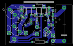
If you move the SPK- to the left of the PGND you will gain some additional space. It might not be as comfortable as having them right next to each other but you only have to do the soldering once. (which will be quite the pain at this size anyway ;-) )
What are the dimensions of the board now? Do you plan on etching it yourself? And what method do you use?
Well then congratulations on your first own Amplifier")
cheers,
hurtz
What are the dimensions of the board now? Do you plan on etching it yourself? And what method do you use?
Well then congratulations on your first own Amplifier
cheers,
hurtz
Thank you all for the help so far
The board now is 45 x 30 mm (if Eagle is not lying). I will let the Speaker - as is now cause the limiting factor is Cin. Now that the concept is clear I will work out the details (traces, additional pads,...).
I never did any etching by myself so I will have to get into that topic. Do you need a lot of equipment? Alternatively I'll have to go to a company...
Final layout and parts list will follow...
I am using toner transfer (because it's cheap) and it took me quite some time to get it working right, now results are good. In retrospect I think invesing in a more professional solution with a 100% reliable outcome would be better. But I guess it depends on your budget and how many PCB's you are making.
My 0.02$
cheers,
hurtz
My 0.02$
cheers,
hurtz
I like that.
Does anyone disagree on any parts of the layout?
I think that the input signal "-" copper should also fill the whole area under the input capacitor, right up to the traces that connect to the cap's ends, to lower the enclosed loop area, to prevent hum and noise pickup. But first I would extend a wide trace from one or both ends of the cap toward the center, in case an input cap with different lead-spacing is desired. At least then there would be someplace to drill new holes and mount it.
And why does it look like the input signal ground reference is tied to the power and speaker ground return to the PSU? If they share a conductor back to the PSU, then the voltages induced across that conductor's inductance (and resistance) by the large capacitor and speaker return currents will modulate the input signal voltage, won't they? Or am I looking at it wrong?
Also, if you could scrunch the two small decoupling/bypass caps under the chip or its pins, or mount them on the bottom of the board, you could move the two large electrolytic caps closer. They need to be as close as possible to the power pins. (And the small caps really should be within a millimeter or two of the pins, at the most, since they are mainly there to prevent high-frequency instability and will not be able to do that otherwise.)
While you're at it, you might as well write some words in copper, to identify your board. Your name and the date come to mind. You can also mark important things like cap and connection polarities, that way.
You should also plan to have a "silkscreen" layer, with just the printing that you want on the board. Put labels for components on there, etc, oriented correctly and not underneath components where they can't be seen after assembly, if possible, etc etc. With toner transfer, you can very-easily put the printing (and even the whole component diagram!) on the top side of the board. I usually did it after I'd etched and drilled everything else, and before soldering or installing anything. Just roughen the surface a little, like you will for the copper side, so the toner will stick better. It's pretty nice to have the component diagram on there. If you can also fit the component labels and values and polarities, etc, it is quite handy during assembly.
My PCB-making page is at Easy PCB (Printed Circuit Board) Fabrication, Using Laser Printer Toner Transfer, with a Household Clothes Iron and Glossy Inkjet Photo Paper; DIY at Home; Better AND Cheaper than Press-n-Peel ( PnP / P-n-P )! Making, Cheap , Economical , fastest fas . You'll have to find the best paper to use, since I haven't done it for a while and they've no doubt changed the model designation by now. Try asking on the Homebrew_PCBs group at yahoogroups.com . Minimal "special" equipment and supplies are needed, the way I liked to do it, except for some blank pcbs (mouser.com, or search for "FR4" on ebay, and now Radio Shack again!) and, probably, a suitable drillpress, with a dremel-like tool strapped to it, and maybe a spring added to take out any "play". But you could actually use HSS "wire gauge" drill bits, available at hardware stores, for so few holes, if you're only going to do this once or twice (or even a regular HSS 1/16th-inch bit, in a pinch). But you might need a small add-on chuck to hold the wire gauge bits, in a regular drill press. The "best way" to do it would be to buy some re-sharpened carbide PCB drill bits, from ebay or the web. But you'd need a high-speed dremel-like rotary tool on a drillpress for those. (And buy a lot of them. They break very easily.)
Other than that, I tried to make sure that there was nothing else that I ever had to order from afar. Use the home-made etchant. It's much better than Ferric Chloride or any of the commercial ones I tried. And it's dirt cheap and available everywhere with no waiting. Just throw some baking soda in it, before you dispose of it.
Last edited:
I think that the input signal "-" copper should also fill the whole area under the input capacitor, right up to the traces that connect to the cap's ends, to lower the enclosed loop area, to prevent hum and noise pickup. But first I would extend a wide trace from one or both ends of the cap toward the center, in case an input cap with different lead-spacing is desired. At least then there would be someplace to drill new holes and mount it.
And why does it look like the input signal ground reference is tied to the power and speaker ground return to the PSU? If they share a conductor back to the PSU, then the voltages induced across that conductor's inductance (and resistance) by the large capacitor and speaker return currents will modulate the input signal voltage, won't they? Or am I looking at it wrong?
...
More drillholes or the extended trace you mentioned is already planned. I started with a large input "-" plane but I believe hurtz mentioned that individual traces might be better (maybe I got him wrong, maybe there a re different opinions).
The input signal ground reference (I believe you refer to Pin 7) is a topic discussed in several threads and I think the outcome was that it should be connected to the Power/Speaker ground and not to the signal "-".
I already took a quick look at your side but probably will have to take some time to work my way through it
More drillholes or the extended trace you mentioned is already planned. I started with a large input "-" plane but I believe hurtz mentioned that individual traces might be better (maybe I got him wrong, maybe there a re different opinions).
I'm sure there are many opinions. But the one best way does exist. I'm not saying that I necessarily know what that is. I'm just indirectly opining about the value of "opinions" (including my own).
Often, the more-difficult part is in trying to actually know (or just decide) whether or not the magnitude of the benefit that might result from using a known best practice or method might be relatively "significant-enough" or not, to make it worth doing it.
In this case, my opinion is that there might be a significant-enough risk and doing it might provide a significant-enough benefit at a low-enough cost, since we're talking about the potential corruption of a high-gain amplifier's input signal.
A "plane" (area fill) would not be strictly necessary, to minimize the enclosed loop (antenna) area between the input + and input - conductors. You could, alternatively, contort the traces' routing so that there is always very little distance between them. But it's usually easier (in most PCB software) and maybe also better to just do a "copper pour" (area fill), instead.
I'm saying that you should do one of those two, since it would, with certainty, provide a possibly-significant-enough benefit and also should not be able to do any harm, and, would be easy-enough to do.
Also, in bringing the input signal and input signal ground conductors to the PCB, you need to be sure to not create any geometric area between them. That means they should either be on shielded twisted pair (with shield connected at input end only, to chassis ground [NOT input signal ground!]), or on unshielded twisted pair, tightly twisted together (5 or 6 turns per inch), ALL the way to each end.
Note, too, that ALL other conductor pairs should also be twisted, or even twisted and shielded, e.g. AC input pair, rectifier-to-smoothing caps pair, power/gnd pairs (or the triple), and output pair. If PCB traces are used for any of those, instead of wires, then the traces should ALWAYS be kept absolutely as close to each other as possible. Otherwise, they will both receive time-varying EM fields and have corresponding currents induced in them, and, transmit time-varying EM fields if they are carrying time-varying currents (both in proportion to the geometric area they enclose, all else being equal). AC Mains and RF (both time-varying EM fields) are almost everywhere, in the air, also.
By the way, I did not notice if you had a low-pass RF filter for your signal input. If not, you need one, or at least need to leave pads and traces for it to be optional.
The input signal ground reference (I believe you refer to Pin 7) is a topic discussed in several threads and I think the outcome was that it should be connected to the Power/Speaker ground and not to the signal "-".
Regardless of how many threads or individuals or opinions were involved, the question is still whether or not that is the correct outcome, and the best plan.
But first, maybe I am confused: I think that "Signal -" and "input signal ground reference" are the same.
My concern was only about how it gets connected to the "zero volts" reference, usually a "star ground" point.
Below is my theory about that, AND my attempted justification. Where is it wrong?
If the conductor that connects the amplifier input's signal ground reference point to the star ground, or to wherever the "zero volts" reference point is, SHARES any part of its length with any other "ground-return" currents except those from the input signal, then it has not been routed the best way, and the sound quality will possibly be degraded (very likely, and significantly, in my opinion).
By "the amplifier input's signal ground reference point", I mean the non-signal or "ground" (i.e. "input -") end of the amp's input resistor (usually connected between amp's input pin and "ground"), the one across which the input signal + and - connect, near the amplifier's input.
A little background, first:
From the power supply, current flows to the amplifier and its decoupling caps, then to the speakers. Some of the AC remnants (ripple) in the voltage cause currents that go straight through the decoupling caps, before getting to the amplifier. They flow back to the power supply through the ground-return conductor. The current that goes to the speakers also comes back, and flows back to the power supply through the same (in your circuit) ground return conductor.
Every conductor has resistance and self-inductance (and capacitance to other conductors but I'm not going to worry about that, here). So all of the mentioned "ground return currents" will be flowing through the power/speaker ground-return conductor, which has inductance and resistance distributed along its length (typically on the order of 10-30 nanoHenries per inch and 1 milliOhm per inch).
Any time-varying current that flows through an inductance will always induce a time-varying voltage across that inductance, according to V = L di/dt, where L is the inductance and di/dt is the time rate-of-change of the current. Likewise, any cirrent flowing through a resistance will induce a voltage across the resistance, according to v = i R.
Now the point:
The point is that the speaker and decoupling capacitor ground-return currents will be very dynamic (versus time) and also quite large in amplitude. So there WILL be a possibly-significant time-varying voltage induced, acoss their ground-return conductor.
That means that back at the non-power-supply end of that conductor, and of every other conductor that shares any of its length, there will be a time-varying voltage, and NOT "zero volts".
If a time-varying voltage is present at the "ground" end of the amplifier's input resistor (which is also called a "bouncing ground"), what will the amplifier 'see"?
Typically, an amplifier sees, as its input, only the difference between the voltages at the two ends of that resistor.
That means that the time-varying voltage at the "ground" end of the input resistor will be arithmetically summed with the input signal, as far as the amplifier is concerned.
That would be "a BAD thing".
That is precisely the reason that "star grounding" was invented. Star grounding is mainly concerned with having separate ground-return conductors for whatever needs them, so that the voltages induced by ground-return currents won't affect other parts of a circuit.
Your PCB should be OK as it is, because you can always disconnect the 10 Ohm resistor and run a separate wire, all the way to the zero-volts reference point, for the input signal ground reference, to compare the resulting sound quality (or to fix the problem, if it's already obvious).
I already took a quick look at your side but probably will have to take some time to work my way through it
It's not as difficult as it might seem. And after you have done it a couple of times, and have everything you need already "on hand", you can go from computer screen to finished PCB in less than one hour. I stopped using those white "plug-in" prototyping boards and just made PCBs; much more reliable.
I am sorry to have blathered-on for so long about all of that. I hope that it made you think and that it might be helpful.
Cheers,
Tom
Last edited:
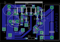
That's not bad!
Probably none of the following is critical.
Maybe you should move the V- connection up close to its capacitor, to try to have the same trace-length to the pins, for both V+ and V-.
And I'm not sure if PGND would be better where it is or between the two big caps. I tend to think it might be better between them. But I could be wrong. Maybe just nearer to them?
Also, sometimes, for the non-ground connection for an electrolytic, it is a good idea to narrow the trace-width, only there at the pad, so that nothing will be able to tend to "go around" the connection to the cap.
I'm sure there are many opinions. But the one best way does exist.
Well I'd like to disagree, as soon as there is more than one variable a best way can only exist to optimize one of the two variables. And with the multitude of variables there are many ways to optimize different aspects that will necessarily lead to different designs (i.e. low noise vs flatness).
If the conductor that connects the amplifier input's signal ground reference point to the star ground, or to wherever the "zero volts" reference point is, SHARES any part of its length with any other "ground-return" currents except those from the input signal, then it has not been routed the best way, and the sound quality will possibly be degraded (very likely, and significantly, in my opinion).
Yes, and can very easily be audible by ground-loops. However it sounds like you are referring to more aspects than the traditional "hum" could you please elaborate?
Maybe you should move the V- connection up close to its capacitor, to try to have the same trace-length to the pins, for both V+ and V-.
And I'm not sure if PGND would be better where it is or between the two big caps. I tend to think it might be better between them. But I could be wrong. Maybe just nearer to them?
While I agree on the "nearer" part, if it means overall distance to the PSU(!) is reduced, I wonder about the "same length". Equal impedance to both caps might seem sensible because with a sinusoidal signal the voltage do for both rails would be the same one could even consider matching the caps for both rails, but since we rarely encounter sinusoidal signal one might question the sensibility of it.
haHA! This is the paper I was looking for. Enjoy!
http://www.x2y.com/filters/TechDay09... _JohnWu.pdf
cheers,
hurtz
Well I'd like to disagree, as soon as there is more than one variable a best way can only exist to optimize one of the two variables. And with the multitude of variables there are many ways to optimize different aspects that will necessarily lead to different designs (i.e. low noise vs flatness).
Ha! Well, at least you're thinking! And like a mathematician, even! But multivariable optimization theory is a thriving field. (My rust-inhibited "gut reaction" follows: ) Obviously, if you want it to be something that "we can do", then you'd just need to first define an optimization metric (cost or benefit function) that incudes all of the variables and aspects that are important to you. Theoretically there might be multiple equally-optimal solution sets, but as you pointed out, some trade-offs might be more-desirable than others. So I'd be tempted to say that our optimization metric was not (and maybe could never be) good-enough and there really would be just one "best" way, by at least a little bit, even if it couldn't be captured by our optimization metric, or ever really even be known, much less decided upon, by us, or even just one of us.
Yes, and can very easily be audible by ground-loops. However it sounds like you are referring to more aspects than the traditional "hum" could you please elaborate?
While I agree on the "nearer" part, if it means overall distance to the PSU(!) is reduced, I wonder about the "same length". Equal impedance to both caps might seem sensible because with a sinusoidal signal the voltage do for both rails would be the same one could even consider matching the caps for both rails, but since we rarely encounter sinusoidal signal one might question the sensibility of it.
haHA! This is the paper I was looking for. Enjoy!
http://www.x2y.com/filters/TechDay09... _JohnWu.pdf
cheers,
hurtz
Sorry, I should have waited until I had more time. I'll get back to the rest of this, soon (next couple of days).
Cheers,
Tom
That layout is pretty much good enough for the task, I'd say.
But that tiny 10R resistor in series with the speaker, what is it supposed to do?
Not very much, we hope. I thought there was a low-value inductor in parallel with it. They are part of the Boucherot network.
hurtz,
Any conductive loop (not just a ground loop!) that has geometric area that it encloses will have a time-varying electric current induced in it by any time-varying magnetic field that shares its space, and the current's amplitude will be proportional to the area enclosed. Also, loops with time-varying currents will create a time-varying magnetic field, similarly. (See Faraday's Law or Maxwell's Equations, if interested.)
In an audio amplifier, loops behave as receiving and/or transmitting antennas, which is one major way that hum and noise (and RF) can get into an amplifier circuit and either affect the sound directly or affect circuit operating points. The induced currents induce voltages across any impedances in the loop, e.g. input resistor, source impedance, even the parasitic impedance of the conductor itself.
So ALL loops should be made to have the minimum enclosed area. The most-typical problematic one is probably the input signal and input signal ground pair. They should at least be tightly twisted together ALL the way from the input jack to the board, and on the board they should always be as close together as possible. Similarly, the AC Mains input pair, transformer secondaries pairs, rectifier to smoothing caps pair(s), power and ground pairs, output pairs, and any I forgot, ideally should all at least be twisted together tightly, all the way from connection to connection, or otherwise be kept as close together as possible, everywhere. They should at least never be separated by any significant distance, especially not by design.
The other phenomenon I mentioned, which you asked me to elaborate on, is a completely-separate mechanism from the loop behavior discussed above, and is the reason for using star grounding:
When a time-varying current flows through a conductor, it induces a voltage across the distributed inductance and resistance of the conductor. The inductance is often particularly bad, since even small-amplitude currents through small inductances, if the current's amplitude is changing fast-enough, can induce large voltages, since the amplitude of V = L di/dt depends on the time-rate-of-change of the current, not its amplitude. Additionally, that voltage is summed with the voltage induced across the distributed parasitic resistance of the conductor, V = iR.
If the conductor is a ground-return conductor in an amplifier, then that makes the "ground" voltage, back at the NON-power-supply end of the conductor, a time-varying voltage(!), i.e. not zero volts relative to the ground reference at the main or star or power supply ground, but a "bouncing" or time-varying "ground" voltage, instead.
If your input signal's ground-reference point, which is usually the "ground" end of a resistor near the amplification device input pins, shares a portion of its ground-connection conductor with the power supply decoupling caps' ground returns or the speaker/output ground return, or any other ground connection, the dynamic ground-return currents from those will induce a voltage across the ground conductor that will appear back at the non-power-supply end of the conductor, and all conductors connected to it, as described above. Then the "ground" end of your input resistor has a time-varying voltage and that voltage will effectively be arithmetically summed with the input signal voltage, as far as the amp inputs are concerned. That would be "a BAD thing".
The ground conductor from the amplifier signal input to the star or main ground should not be shared by any other parts of the circuit.
First, impedance is actually a general concept that is not retricted to sinusoidal signals, in any way. (And even if it were, basically ALL signals can be decomposed into a summation of sinusoidal components, so it would still apply.)
And distance to the PSU is much less important if we implement the decoupling caps very well. They act much like local point-of-load power supplies, for basically all of the transient signals; anything that changes too fast for the main psu's current to make it through the inductance in the main supply rails, in time. If the psu is more than a few centimeters distant, it might as well be a meter.
Anyway, my thinking was simply to have symmetric power input characteristics, so that their responses would be more matched. The power supply and ground trace distances involved will affect both impedance and timing. If one is longer, it will have more inductance and the transient response will have different timing and shape characteristics (both amplitude and phase angle versus time will be different), just as one example.
The only real question is about how significant the effects of any differences might be. For most people, it would be quicker and easier to just make them as similar as possible in length and size etc, than to try to figure out whether or not it might matter. In my case, I would not leave them asymmetrical unless I had actually proven to myself that any degradation would be truly negligible.
The link does not work. It needs to be pasted in as a complete link, rather than from the compacted version that already had the ellipsis (the "...") in it.
Regards,
Tom
<snipped>
Yes, and can very easily be audible by ground-loops. However it sounds like you are referring to more aspects than the traditional "hum" could you please elaborate?
Any conductive loop (not just a ground loop!) that has geometric area that it encloses will have a time-varying electric current induced in it by any time-varying magnetic field that shares its space, and the current's amplitude will be proportional to the area enclosed. Also, loops with time-varying currents will create a time-varying magnetic field, similarly. (See Faraday's Law or Maxwell's Equations, if interested.)
In an audio amplifier, loops behave as receiving and/or transmitting antennas, which is one major way that hum and noise (and RF) can get into an amplifier circuit and either affect the sound directly or affect circuit operating points. The induced currents induce voltages across any impedances in the loop, e.g. input resistor, source impedance, even the parasitic impedance of the conductor itself.
So ALL loops should be made to have the minimum enclosed area. The most-typical problematic one is probably the input signal and input signal ground pair. They should at least be tightly twisted together ALL the way from the input jack to the board, and on the board they should always be as close together as possible. Similarly, the AC Mains input pair, transformer secondaries pairs, rectifier to smoothing caps pair(s), power and ground pairs, output pairs, and any I forgot, ideally should all at least be twisted together tightly, all the way from connection to connection, or otherwise be kept as close together as possible, everywhere. They should at least never be separated by any significant distance, especially not by design.
The other phenomenon I mentioned, which you asked me to elaborate on, is a completely-separate mechanism from the loop behavior discussed above, and is the reason for using star grounding:
When a time-varying current flows through a conductor, it induces a voltage across the distributed inductance and resistance of the conductor. The inductance is often particularly bad, since even small-amplitude currents through small inductances, if the current's amplitude is changing fast-enough, can induce large voltages, since the amplitude of V = L di/dt depends on the time-rate-of-change of the current, not its amplitude. Additionally, that voltage is summed with the voltage induced across the distributed parasitic resistance of the conductor, V = iR.
If the conductor is a ground-return conductor in an amplifier, then that makes the "ground" voltage, back at the NON-power-supply end of the conductor, a time-varying voltage(!), i.e. not zero volts relative to the ground reference at the main or star or power supply ground, but a "bouncing" or time-varying "ground" voltage, instead.
If your input signal's ground-reference point, which is usually the "ground" end of a resistor near the amplification device input pins, shares a portion of its ground-connection conductor with the power supply decoupling caps' ground returns or the speaker/output ground return, or any other ground connection, the dynamic ground-return currents from those will induce a voltage across the ground conductor that will appear back at the non-power-supply end of the conductor, and all conductors connected to it, as described above. Then the "ground" end of your input resistor has a time-varying voltage and that voltage will effectively be arithmetically summed with the input signal voltage, as far as the amp inputs are concerned. That would be "a BAD thing".
The ground conductor from the amplifier signal input to the star or main ground should not be shared by any other parts of the circuit.
While I agree on the "nearer" part, if it means overall distance to the PSU(!) is reduced, I wonder about the "same length". Equal impedance to both caps might seem sensible because with a sinusoidal signal the voltage do for both rails would be the same one could even consider matching the caps for both rails, but since we rarely encounter sinusoidal signal one might question the sensibility of it.
First, impedance is actually a general concept that is not retricted to sinusoidal signals, in any way. (And even if it were, basically ALL signals can be decomposed into a summation of sinusoidal components, so it would still apply.)
And distance to the PSU is much less important if we implement the decoupling caps very well. They act much like local point-of-load power supplies, for basically all of the transient signals; anything that changes too fast for the main psu's current to make it through the inductance in the main supply rails, in time. If the psu is more than a few centimeters distant, it might as well be a meter.
Anyway, my thinking was simply to have symmetric power input characteristics, so that their responses would be more matched. The power supply and ground trace distances involved will affect both impedance and timing. If one is longer, it will have more inductance and the transient response will have different timing and shape characteristics (both amplitude and phase angle versus time will be different), just as one example.
The only real question is about how significant the effects of any differences might be. For most people, it would be quicker and easier to just make them as similar as possible in length and size etc, than to try to figure out whether or not it might matter. In my case, I would not leave them asymmetrical unless I had actually proven to myself that any degradation would be truly negligible.
haHA! This is the paper I was looking for. Enjoy!
http://www.x2y.com/filters/TechDay09... _JohnWu.pdf
cheers,
hurtz
The link does not work. It needs to be pasted in as a complete link, rather than from the compacted version that already had the ellipsis (the "...") in it.
Regards,
Tom
Last edited:
- Status
- This old topic is closed. If you want to reopen this topic, contact a moderator using the "Report Post" button.
- Home
- Amplifiers
- Chip Amps
- One more LM3886 PCB