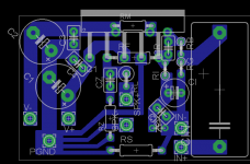
Hello everybody,
I've read through a lot of threads regarding the LM3886 and wanted to do a layout of my own.
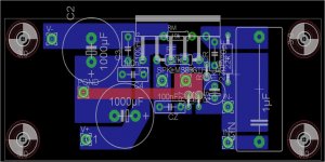
Here it is:

Rm (10k) and Rf (22k) will be soldered directly to the pins
Rz = 2R7, Cz = 100nF
Rg = 22k
Ri = 1k, Ci = 22µF
Cr = 220pF
Rs = 10R
At the moment all resistors are 1/4W, should any of them be bigger (e.g. Zobel)?
Any comments, mistakes I've made, parts I forgot, things that could be improved?
I've read through a lot of threads regarding the LM3886 and wanted to do a layout of my own.
Here it is:
Rm (10k) and Rf (22k) will be soldered directly to the pins
Rz = 2R7, Cz = 100nF
Rg = 22k
Ri = 1k, Ci = 22µF
Cr = 220pF
Rs = 10R
At the moment all resistors are 1/4W, should any of them be bigger (e.g. Zobel)?
Any comments, mistakes I've made, parts I forgot, things that could be improved?
Ok, a few things I noticed:
- Why is Cr physically so big?
- You might want to remove the vlaues of the components from your design so it will be easier to read.
- Have you read through the LM3886 datasheet? Also the LM4780 is a good read and has more detailed information than the lm3886 datasheet. (The lm4780 is two lm3886 in one housing)
- Combining a classic PCB with p2p (point to point) components is not considered to be "nice". Although there is no technical problem with that, you will have a lot of work whith those p2p components, and the question arises why not to make it a complete p2p amp.
- Why are C3/C4 the size they are?
- You can use a protection diode across Ci
- Do you already have a PSU?
cheers!
hurtz
Hello,
thanks for the reply:
- Cr is so big because I didn't find the right model in Eagle
- will do
- Did read through the LM3886, will read the lm4780
- I already made a complete P2P amp and didn't like it to much (handling) that's why I want to make a hybrid version
- Values for C3/C4 are like most of the other layouts
- What kind of diode would be suitable and what exactly shall it protect from?
- Yes, PSU is available (either single rectifier and 2x3300µF per rail (monoblock use) or dual rectifier and 3x4700µF+10000µF per Rail for stereo use). All Caps bridged with 0,1µF film, all diodes bridged with 0,033µF.
Attachments
Hi,
- Sorry I meant C1/C2 with 1000uF. Although you will achieve a slightly lower ESR of 0r04 as opposed to a 220uF with 0r09 (reichelt 105° elkos). But considering the physical size, a smaller capacitor might be placed closer to the lm and overall impedance might be reduced a bit further. So if you don't have a very long connection from the PSU to the amp a little less capacitance should work well.. since the datasheet suggests 10uF in any case.
- Cr should also be available as 2.5mm if you want to keep the size down.
- The diode protects Ci in case of power supply failure, in general i think also it is not needed but it adds a little extra layer of security. 1n4001 or something like that.
- Elliott Sound Products - Linear Power Supply Design this is a good source to get some info on PSU design. Or to make it short: 1VA for the transformer per 1W output power. Many small capacitors for the psu are better than one large capacitor. and 10.000uF per rail should be more than enough. I am using one PSU with 3 x 4700uF per rail for a stereo steup. A good test of the PSU is to connect one (two) analog voltmeters to each rail and then watch the voltage drop under heavy load. (I got a maximum of 3V with an 80VA 18V toroid).
- Also you might want to consider not using ground planes but individual traces to keep the grounds better separated (also helps readability ;-)). Also think of the traces as having their own very real resistances and electrons being rather slow. I'm thinking specifically of Cz which is placed after the speaker out. I have no idea what the impact of this is, maybe one of the experts around here might elaborate on this?
- Consider using a 47pF cap across the RCA input jack, helps RF noise. Around 330pF or less across Rin, again for RF filtering. Those two gave me a good 3dB decrease in noise.
- Get familiar with Rightmark Audio Analyzer (rmaa, free tool) and your soundcard. This will help you a lot when debugging possible issues, and it is also nice for everyone else around here to see some measurements. Especially since a lot of borderline audible effects can be made visible. I'm not saying a graph will tell how good the listening experience is, but it will definitly help you find any issues you might have.
cheers!
hurtz
Hello,
- Size can be reduced to 10 mm or 8 mm diameter (depending on capacity and voltage), since I will be using a 2x18V toroid, 35V should be fine. I will take a look at the PCB and choose between 220µF (8 mm) or more (10 mm).
- Found lots of them with 2,5 mm, don't know why I didn't find them before.
- Will be included
- Will check this when the amp is done, guess I'll start with the smaller units.
- Will make a different version with modified ground traces (as proposed).
- Will consider that
- Will do.
Next step:
Work my way through your thread, modifiy everything, come back")
Might take some time since I'm pretty busy the next few weeks.
- Size can be reduced to 10 mm or 8 mm diameter (depending on capacity and voltage), since I will be using a 2x18V toroid, 35V should be fine. I will take a look at the PCB and choose between 220µF (8 mm) or more (10 mm).
- Found lots of them with 2,5 mm, don't know why I didn't find them before.
- Will be included
- Will check this when the amp is done, guess I'll start with the smaller units.
- Will make a different version with modified ground traces (as proposed).
- Will consider that
- Will do.
Next step:
Work my way through your thread, modifiy everything, come back
Might take some time since I'm pretty busy the next few weeks.
Hello again,
after reading through the datasheets and Hurtzs thread I modified some things.
Rf will still be soldered directly to the Chip. Rm will either be soldered to the chip or placed under it.
I probably will add a small ceramic cap across the Input socket (22 - 47pF).
Ri and Ci give a frequency of ~7,3 Hz, Cin and Rin ~2,8 Hz, so this should be ok.
Since Ri = Rb and Rg = Rf I omitted Rf1 and Cf.
I am not sure about the ground stars, should I leave it like that or try to make it more star-like?
What about the rest (width of traces etc.)?
Other suggestions regarding layout or parts?
EDIT: OK, stupid me, forget the jumper, will be placed bit lower as a normal trace...
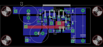
Parts list:
Cin = 1 µF (MKP)
Ci = 56 µF (electrolytic, 35V)
Cz = 100 nF (Wima MKS-02)
C1/2 = 470 µF (Panasonic FC, 35V)
C3/4 = 100 nF (Wima MKS-02)
Cib = 100 nF (Wima MKS-02)
Cr = 22 pF (ceramic)
Rb = 1k
Ri = 1k
Rg = 22k
Rf = 22k
Rm = 10k
Rz = 2R7
Rs = 10R
all metal or carbon, 1/4W.
Rl = 10R + ~0,6 mH (MOX, 2W)
D1 = 1N4001
after reading through the datasheets and Hurtzs thread I modified some things.
100nF Cap across Ci (from datasheet)- Diode across Ci for protection
- Values for C1/C2 reduced from 1000 µF to 470µF in order to gain place
- Tried to build up two ground stars, one for low-level and one for high level signals
Rf will still be soldered directly to the Chip. Rm will either be soldered to the chip or placed under it.
I probably will add a small ceramic cap across the Input socket (22 - 47pF).
Ri and Ci give a frequency of ~7,3 Hz, Cin and Rin ~2,8 Hz, so this should be ok.
Since Ri = Rb and Rg = Rf I omitted Rf1 and Cf.
I am not sure about the ground stars, should I leave it like that or try to make it more star-like?
What about the rest (width of traces etc.)?
Other suggestions regarding layout or parts?
EDIT: OK, stupid me, forget the jumper, will be placed bit lower as a normal trace...
Parts list:
Cin = 1 µF (MKP)
Ci = 56 µF (electrolytic, 35V)
Cz = 100 nF (Wima MKS-02)
C1/2 = 470 µF (Panasonic FC, 35V)
C3/4 = 100 nF (Wima MKS-02)
Cib = 100 nF (Wima MKS-02)
Cr = 22 pF (ceramic)
Rb = 1k
Ri = 1k
Rg = 22k
Rf = 22k
Rm = 10k
Rz = 2R7
Rs = 10R
all metal or carbon, 1/4W.
Rl = 10R + ~0,6 mH (MOX, 2W)
D1 = 1N4001
Attachments
Last edited:
I don't understand why you have added these.................
100nF Cap across Ci (from datasheet)- Diode across Ci for protection
..........
I don't understand why you have added these.
Hello master
the 100nF Cap comes from the LM4780 application note (page 19 - high performance considerations), the diode was proposed by you in the thread of hurtz ("The yet tiniest single-sided LM3886?" - post #196)
The NFB cap has virtually no AC voltage and virtually no DC voltage across it when the amplifier is working properly.
That's why the single diode does not interfere with normal audio operation.
Adding a second inverse parallel diode will similarly have no impact on the audio operation. The diodes are there to limit damaging voltages if or when the amplifier misbehaves.
The suggested inverse parallel diodes across the 10r are also there to limit damaging voltages, if the amplifier, or one of the connected sources misbehaves.
Hi,
good progress!
A few minor changes maybe:
- the square copper pour area in the top right corner, currents demands arrent very high on the input. I have once read a paper on electron flow through copper areas where it was visualised where the most electrons are at. theory suggests that the bigger the cable diameter, the less the resistance, but in a copper plane which is more or less 2 dimensional, for an electron to use a different than the direct path it has to travel a significantly longer distance i.e. more resistance. so the top left corner of the top right pour area will never be used. This is how I would explain it, please someone correct me if I'm wrong... I'm not a physicist..
The worst thing that could happen is an increased antenna area, but since the board is very small I doubt it will make a difference.
- Why are there 2 Power grounds? You could/should make the MAG one star point (not necessarily the shape) so just put the speaker return directly adjecent to it (same goes for low level). Also since the different traces of returns are seperated up to a point, you might as well keep them separated until they meet at the MAG. Otherwise you might provoke gound loops. Also if you already join the two coils of the toriod on the psu i.e. create the gnd level, speaker/low-level etc. can be returned directly to the psu (this is debated however, mostly for low level). I solved this by simply creating the gnd on the AMP itself. This is only slightly overshadowed by the fact that I use one PSU for two amps.
- If using more than one channel, you might think of elevating the low level return by a 10r or something.
- More of a technical thing, try to let wires cross at 90° angles to minimize inductance. Looking at the low level jumper and lm3886 gnd pin.
cheers!
hurtz
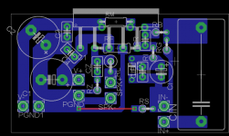
I like the way that the -IN input trace and components follow the line of the +IN input via that DC blocking capacitor. Minimises loop area. Add some alternative Pin Pitch pads for this cap. Similar add optional pads for PIN Pitch for as many other caps as there is space to allow.
Can you see the land on the Power Ground in between the four decoupling capacitors? Could this land be expanded slightly to provide a Pad for a connection. Keep the components where they are, just expand the land.
Now, can you find an alternative route for Rz? Keep Cz where it is and connect Rz to that PG land. Is there a way to implement this? What I am trying to do for you is reduce the impedance of the Zobel route so that the VHF that this component is trying to provide a load for, is actually implemented.
I don't like the thin trace for SPK Return.
This could be eliminated and instead use the Main Audio Ground that will be off the PCB. The MAG can even be the SPK Return Terminal on the back panel. That then requires no additional pad for the SPK Return.
Last edited:
I already thougth of adding additional pads for allowing the use of different Cins. Probably should implement them.
Do you mean the land between C1-C4? Probably can access this area with a Top-Layer trace or I could try to change the position of C1 (bit lower) and lead Rz between C1 and C4.
Ok, will rework the SPK Return, probably as proposed by you.
Do you mean the land between C1-C4? Probably can access this area with a Top-Layer trace or I could try to change the position of C1 (bit lower) and lead Rz between C1 and C4.
Ok, will rework the SPK Return, probably as proposed by you.
- Status
- This old topic is closed. If you want to reopen this topic, contact a moderator using the "Report Post" button.
- Home
- Amplifiers
- Chip Amps
- One more LM3886 PCB