Fliege notch filter series resistor works after all..
Turns out I was wrong in my post above about adding a small series resistance to the center 0.047uF cap affecting the filter's Q and notch depth. I just handn't turned the frequency adjust pot far enough yet to fully null it. Took about 5 turns from the center on the 20 turn pot, which was centered when I installed it. Also turned out that only 4.99 ohms is needed to isolate that 0.047uF cap from the op amp output, not 20 ohms. So the other isolation method above, the BUF634 chip added to the inner op amp, really isn't needed since this simple resistor trick does the job.
The LT Spice simulation comes within the ballpark of matching the real-word results, if the 27R resistors are changed to 2R to shift the frequency to match the pot turn. The simulation gives around 2.4mV out with 200mV in at the notch frequency, or 20log(2.4/200) = -38dB. The real world results shown on the DMMs below are 0.97mV out with 37mV in, or -31.6dB. The pre-amp (not yet populated) on the Fliege notch filter board is set for +33dB. So the net result would be to restore the fundamental to its original level, but boost all the device harmonics by 33dB, useful for looking at the harmonics on a scope's FFT.
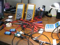
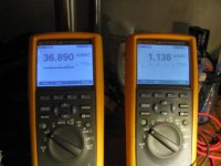
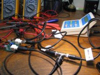
* The first two photos show the test setup. I'm using DMMs instead of the scope to get more accurate absolute values.
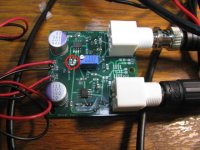
* The next photo shows the series resistor modification in the red circle. Just a 4.99R 1206 resistor put in series with the 0.047uF 1206 capacitor. The resistor isolates the capacitive load from the output of the LME49990 and restores the waveshape. The other LME49990 doesn't have that problem in the circuit. The board now has the proper filter caps on the power supply and BNCs after another bunch of parts from Mouser.
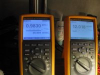
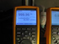
* The next two photos show in the input signal from the generator, 37mV, and the output from the Fliege notch filter, 0.97mV = -31.6dB. The pot is adjusted for maximum null, about 5 turns from center with the 2 27R frequency set resistors in place. The second photos shows the frequency out of the generator, 999.96Hz.
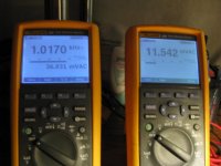
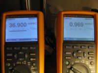
* The next two photos are a test of notch wall width and symmetry. These are +/-1Hz from the 1kHz (1001 Hz and 999Hz).
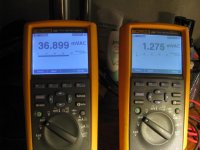
* The final two photos are the same thing, a notch width and symmetry test, but I'm shooting for -10dB here, up from the notch bottom's -31.6dB. This happened at +/-17Hz from the 1kHz Fc, as the meters show. 11.5mV on one side of the notch wall and 12.0mV on the other, reasonably symmetrical.
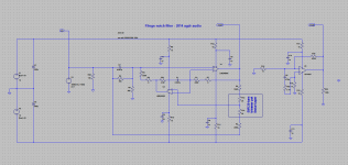
* The schematic has the 4.99 isolation resistor now in series with the circuit's middle 0.047uF cap.
Turns out I was wrong in my post above about adding a small series resistance to the center 0.047uF cap affecting the filter's Q and notch depth. I just handn't turned the frequency adjust pot far enough yet to fully null it.
Took about 5 turns from the center on the 20 turn pot, which was centered when I installed it. Also turned out that only 4.99 ohms is needed to isolate that 0.047uF cap from the op amp output, not 20 ohms. So the other isolation method above, the BUF634 chip added to the inner op amp, really isn't needed since this simple resistor trick does the job.The LT Spice simulation comes within the ballpark of matching the real-word results, if the 27R resistors are changed to 2R to shift the frequency to match the pot turn. The simulation gives around 2.4mV out with 200mV in at the notch frequency, or 20log(2.4/200) = -38dB. The real world results shown on the DMMs below are 0.97mV out with 37mV in, or -31.6dB. The pre-amp (not yet populated) on the Fliege notch filter board is set for +33dB. So the net result would be to restore the fundamental to its original level, but boost all the device harmonics by 33dB, useful for looking at the harmonics on a scope's FFT.
* The first two photos show the test setup. I'm using DMMs instead of the scope to get more accurate absolute values.
* The next photo shows the series resistor modification in the red circle. Just a 4.99R 1206 resistor put in series with the 0.047uF 1206 capacitor. The resistor isolates the capacitive load from the output of the LME49990 and restores the waveshape. The other LME49990 doesn't have that problem in the circuit. The board now has the proper filter caps on the power supply and BNCs after another bunch of parts from Mouser.
* The next two photos show in the input signal from the generator, 37mV, and the output from the Fliege notch filter, 0.97mV = -31.6dB. The pot is adjusted for maximum null, about 5 turns from center with the 2 27R frequency set resistors in place. The second photos shows the frequency out of the generator, 999.96Hz.
* The next two photos are a test of notch wall width and symmetry. These are +/-1Hz from the 1kHz (1001 Hz and 999Hz).
* The final two photos are the same thing, a notch width and symmetry test, but I'm shooting for -10dB here, up from the notch bottom's -31.6dB. This happened at +/-17Hz from the 1kHz Fc, as the meters show. 11.5mV on one side of the notch wall and 12.0mV on the other, reasonably symmetrical.
* The schematic has the 4.99 isolation resistor now in series with the circuit's middle 0.047uF cap.
Attachments
-
 IMG_2376.JPG75.8 KB · Views: 238
 -
 IMG_2386.JPG48.1 KB · Views: 33
 -
 IMG_2385.JPG47.9 KB · Views: 49
 -
 IMG_2383.JPG53.6 KB · Views: 31
 -
 IMG_2382.JPG48.6 KB · Views: 34
 -
 IMG_2381.JPG32.4 KB · Views: 218
 -
 IMG_2380.JPG46.4 KB · Views: 229
 -
 IMG_2379_1.jpg99.7 KB · Views: 233
 -
 IMG_2377.JPG84 KB · Views: 247
 -
 Fliege notch filter circuit 1.png26.3 KB · Views: 42
Last edited:
Hi Agdr, can you please confirm a couple of things for the V3 board,
-Is the positive end of C16 closest to the edge of board?
-When running the power management circuit in the stock config with R13 and no R14 does it need the jumper cable, or is that only for the modified version with no R13 and a diode across R14?
If anybody in the UK has a stash of 2N7002LT1G fets i would really appreciate a couple. I somehow forgot to put them into my last Mouser order
Hi Agdr, can you please confirm a couple of things for the V3 board,
-Is the positive end of C16 closest to the edge of board?
That is correct, the banded end goes closest to the board edge. Any other type of capacitor would have the band on the negative end, but on those SMD tantalums the banded end is positive. I just noticed in looking at the layout that I didn't put the additional text about the banded end on that capacitor, just the band on the symbol. I'll add that on the next board run in a few weeks.
-When running the power management circuit in the stock config with R13 and no R14 does it need the jumper cable, or is that only for the modified version with no R13 and a diode across R14?
That is right, no cable needed in that case. You will still get a small amount of turn-off thump though, although I measured it in one of the posts above to be greatly reduced. Removing R13, adding the zener for R14 and adding the cable will give you zero turn off thumps.
If anybody in the UK has a stash of 2N7002LT1G fets i would really appreciate a couple. I somehow forgot to put them into my last Mouser order
I'll drop a couple in an envelope, no charge.
They are so small they would fit in a regular letter envelope. I need to send two transistors out to another builder anyway who bought a parts kit, since I screwed up and sent him a strip of 3 with 2 already missing from the strip. In fact, I'll drop a zener for "R14" in too and you can give that zero thump mod a try if you want. I'll get those in the mail tomorrow.
Last edited:
mcandmar - I just remembered something. C16 is a capacitor you probably won't want to install. That capacitor is just in parallel with C7 to create an (optional) much longer turn-on delay for the relay if someone wanted. The 10uF C7 is providing about 5 seconds worth of delay, which is probably fine for most folks. Adding C16 would bump that up to around 45 seconds. For a longer delay replacing C7 with a 22uF Mouser #810-C3216X5R1V226M would roughly double the turn-on delay to 10 seconds.
I should probably leave the pads for C16 off entirely on the next board spin. I originally put C16 on the board to provide some flexibility in testing different turn-on delay times.
I should probably leave the pads for C16 off entirely on the next board spin. I originally put C16 on the board to provide some flexibility in testing different turn-on delay times.
Last edited:
45 seconds does sound a bit much so i'll pull that capacitor off again, i just ordered everything in the BOM (or so i thought).
One bit of constructive criticism, the orientation of the diodes, LED's and tants isn't that clear so i had to refer to your pictures to verify i had them the right way around. Rather than the little dots can you make them a vertical line under each component so its more obvious. Would also be worth noting the position of the relay on the bottom of the board, only reason i knew that was from seeing a picture you had posted previously, most people would assume it goes topside. Or does it matter?
Thanks for the parts offer Agdr, you are a true gentleman
Ok, I put mine together over the last 2 days.
Left channel gives a "pop" when turned on, (when the relay clicks on?) no input present
volume of music after that is very low.
Right channel seems to be good. No pop when turned on, music starts playing at what seems to be normal level.
Both LED's light up at the same time.
did not modify the O2 board as of yet. It did work fine before the addition of the O2 Booster Board.
This is using the battery only.
Reverted back, and everything works normaly.
I am going to be going over the solder points, and reflowing them, Any idea on which ones to concentrate on, since it is the left channel?..
I am going to be going over the solder points, and reflowing them, Any idea on which ones to concentrate on, since it is the left channel?..
Double check the orientation of the two opamps, or post a pic in case we can spot something..
Hi, I started to put my board together and have a question. D2 is not marked for a direction on the board. Which way does it go?
Thanks
Same as D1.
@agdr: Recived the transistors and diodes on friday, thanks again for those, i'm going to try and finish it off over the weekend
Good work guys! I'm glad to see booster boards getting sucessfully completed.
That is right, D1 and D2 go with the band towards K1, away from the board edge. If you do the "no-thump" modification (remove R13, put a zener in "R14". and the wire from one R13 pad to the O2 board) that zener in the "R14" postion goes with the band toward the edge of the board, opposite of D2 (same type of zener diode for both though).
That is right, D1 and D2 go with the band towards K1, away from the board edge. If you do the "no-thump" modification (remove R13, put a zener in "R14". and the wire from one R13 pad to the O2 board) that zener in the "R14" postion goes with the band toward the edge of the board, opposite of D2 (same type of zener diode for both though).
As I also just shared on head-fi, thanks to some very gracious trouble shooting help from agdr (hint: having a diode in the wrong orientation in R14 is a bad plan), I'm very pleased to report that I got my O2 booster board (v.3.0) up and running today! I also subbed in the optional dual LME49990 adaptor in place of the stock gain chip, bringing the amp's slew rate up to a respectable 20V/us.
I'm very happy with the results thus far! As promised, DC offset is now essentially nonexistent per my cheap meter, turn on/off thump is eliminated, and the overall sound does seem to have improved in a couple of subtle respects to my ears. While acknowledging that this all may be attributable to the delusions of my heat oppressed brain (thanks Shakespeare and Hume!), I could swear that the minor treble glare I occasionally perceived in the O2 has vanished and the deep bass seems just a little bit more present. For example, I have a great recording of traditional Anglican choral and pipe organ music that was made a few years back in the renowned St. Martin-in-the-Fields Cathedral (on Trafalgar Square) - Amazon.com: Chorales & Preludes: Music . The organ, in particular, always sounded just the tiniest bit thin on my stock self-built O2 (relative to my mainline and also the live evensong services I made a point of attending at that Cathedral while traveling - the acoustics in which are arguably the best in the world for choral music). With agdr's booster and the LME49990 adaptor in place, my AD's seem to be singing this music back just a bit closer to the sound of live.
I think I'm going to have to build up my spare O2 board and related components so I can actually A/B rapidly between the stock and modified amps, but as noted by one or two others in the head-fi thread, agdr's board truly does seem to result in subjective as well as objective improvements!
Thanks again for all your efforts in designing and supporting such a cool project agdr! I stand by my offer of as many beers as you can put down in an evening if you venture out towards LA at some point.
I have yet to drill the holes in my front panel for the booster board LED's, but here are a few pics showing her up and running. Note that the LED in R14 is in the wrong orientation in my first pic below, so if you're a builder, don't mimic me there!
-Mike
I'm very happy with the results thus far! As promised, DC offset is now essentially nonexistent per my cheap meter, turn on/off thump is eliminated, and the overall sound does seem to have improved in a couple of subtle respects to my ears. While acknowledging that this all may be attributable to the delusions of my heat oppressed brain (thanks Shakespeare and Hume!), I could swear that the minor treble glare I occasionally perceived in the O2 has vanished and the deep bass seems just a little bit more present. For example, I have a great recording of traditional Anglican choral and pipe organ music that was made a few years back in the renowned St. Martin-in-the-Fields Cathedral (on Trafalgar Square) - Amazon.com: Chorales & Preludes: Music . The organ, in particular, always sounded just the tiniest bit thin on my stock self-built O2 (relative to my mainline and also the live evensong services I made a point of attending at that Cathedral while traveling - the acoustics in which are arguably the best in the world for choral music). With agdr's booster and the LME49990 adaptor in place, my AD's seem to be singing this music back just a bit closer to the sound of live.
I think I'm going to have to build up my spare O2 board and related components so I can actually A/B rapidly between the stock and modified amps, but as noted by one or two others in the head-fi thread, agdr's board truly does seem to result in subjective as well as objective improvements!
Thanks again for all your efforts in designing and supporting such a cool project agdr! I stand by my offer of as many beers as you can put down in an evening if you venture out towards LA at some point.
I have yet to drill the holes in my front panel for the booster board LED's, but here are a few pics showing her up and running. Note that the LED in R14 is in the wrong orientation in my first pic below, so if you're a builder, don't mimic me there!
An externally hosted image should be here but it was not working when we last tested it.
An externally hosted image should be here but it was not working when we last tested it.
An externally hosted image should be here but it was not working when we last tested it.
-Mike
I also subbed in the optional dual LME49990 adaptor in place of the stock gain chip, bringing the amp's slew rate up to a respectable 20V/us.
I must have missed that memo, are the details in this thread?
I must have missed that memo, are the details in this thread?
Hey mcandmar - yeah, agdr discussed it briefly here (see post no. 119), and there was a bit more back and forth on the topic on head-fi (see post no. 2149 et seq. on this page: O2 AMP + ODAC - Page 144).
Hey mcandmar - yeah, agdr discussed it briefly here (see post no. 119), and there was a bit more back and forth on the topic on head-fi (see post no. 2149 et seq. on this page: O2 AMP + ODAC - Page 144).
Excellent thank you, will add a few to my Mouser basket
Excellent thank you, will add a few to my Mouser basket
No problem! The ebay adaptors actually come with the dual LME49990's preinstalled. Not sure what mouser's pricing is like by comparison if you were to buy an upopulated adaptor, but here's the seller I went with: Dual SOIC LME49990 DIP8 Adapter | eBay
DubiousMike: Congratulations on the build! I'm glad flippiing that diode solved it. Thanks for the listening update too.
On the next run of booster boards I'm going to make that no-thump modification standard. I'll have an official diode symbol in for "R14" and R13 will just become a hole to run the wire to the O2 board. I'm also going to eliminate the pad for C16, the extra parallel timing capacitor, since the small one in for C17 is providing more than enough delay.
Please do post what you think when you try A/B'ing with the stock O2! Something I'm waiting for is when someone with better critical listening ears than mine eventually builds up booster boards with both the OPA140 in one and OPA827 in the other, then A/B's those. The OPA140 should produce slightly lower DC offset numbers, 20uV vs 200uV (still 10x better than the stock O2 headamp), while the OPA827 has slightly better AC numbers (distortion, noise) as per the datasheet. Will be interestinng to hear if the consensus is any audible difference or not.
macanmar: that "stuffed" eBay dual LME49990 adaptor fits in the O2 board just fine. I've tried it. If you get that one though make sure it is the dual one. That vendor also sells a single chip LME49990 adaptor.
I always worry a bit about the eBay stuff being a fake, but that vendor has been around a while and it is shipping from here and not China. Plus the LME49990 are fairly cheap these days - $2.50 in 100 quantity at Mouser - so probably less motivation for them to use fakes. That pricing is interesting. A year ago Mouser was selling those chips for $2.30 for just a single chip! Now I see their single chip price is up to $3.50.
Thanks for the listening update too.On the next run of booster boards I'm going to make that no-thump modification standard. I'll have an official diode symbol in for "R14" and R13 will just become a hole to run the wire to the O2 board. I'm also going to eliminate the pad for C16, the extra parallel timing capacitor, since the small one in for C17 is providing more than enough delay.
Please do post what you think when you try A/B'ing with the stock O2! Something I'm waiting for is when someone with better critical listening ears than mine eventually builds up booster boards with both the OPA140 in one and OPA827 in the other, then A/B's those. The OPA140 should produce slightly lower DC offset numbers, 20uV vs 200uV (still 10x better than the stock O2 headamp), while the OPA827 has slightly better AC numbers (distortion, noise) as per the datasheet. Will be interestinng to hear if the consensus is any audible difference or not.
macanmar: that "stuffed" eBay dual LME49990 adaptor fits in the O2 board just fine. I've tried it. If you get that one though make sure it is the dual one. That vendor also sells a single chip LME49990 adaptor.
I always worry a bit about the eBay stuff being a fake, but that vendor has been around a while and it is shipping from here and not China. Plus the LME49990 are fairly cheap these days - $2.50 in 100 quantity at Mouser - so probably less motivation for them to use fakes. That pricing is interesting. A year ago Mouser was selling those chips for $2.30 for just a single chip! Now I see their single chip price is up to $3.50.
Thanks Agdr but i have already ordered a bunch of adapters from eBay for another project so i will just source the chips directly from Mouser.
Have you had any thoughts on local power supply bypass caps, i was just reading this section on the datasheet which has me wondering if they should be added to the adapter board.
"To achieve a low noise and high-speed audio performance, power supply bypassing is extremely important. Applying multiple bypass capacitors is highly recommended. From experiment results, a 10μF tantalum, 2.2μF ceramic, and a 0.47μF ceramic work well."
Looking at the schematic there is only a .22uf from + and - to ground, and a single .22uf across the + and -. The later of which is the only one physically near U1.
Have you had any thoughts on local power supply bypass caps, i was just reading this section on the datasheet which has me wondering if they should be added to the adapter board.
"To achieve a low noise and high-speed audio performance, power supply bypassing is extremely important. Applying multiple bypass capacitors is highly recommended. From experiment results, a 10μF tantalum, 2.2μF ceramic, and a 0.47μF ceramic work well."
That is a very interesting point! This is going to be one of my long-winded answers since it relates directly to the next version of the booster board.
That decoupling issue is the first thing I checked with the adaptor board. No oscillations out to the 200mHz bandwidth of the scope, so everything works out. Ideally those bypass caps should be added to prevent any chance of oscillation. But NwAvGuy did an excellent job with the layout and even that much higher speed chip is working OK. Part of that is he very effectively star grounded the input gain stage section separately from the output section. I've done a similar thing with the ODA amp.
Where additional trouble can come in is with capacitive loads. But in this case since that LME49990 chip is used "internally" in the O2, always powering the volume control, there are no variable output loads. So probably by luck as much as by design that adaptor board actually works in the circuit that was never intended to deal with a chip that fast.
I haven't said much about it, but adding additional power supply decoupling to the booster board was a very important thing, given the additional lead lengths (inductance) to get the signals to and from that remote add-on board. Also given the faster (greater gain bandwidth product) OPA140 and much faster OPA827 and the LME49990 output chips. Those two large yellow 47uf tantalum caps, C1 and C2, take the place of the 10uf tantalum in the design note. Since those larger caps are for preventing lower frequency oscillations one set per a small board like that does the job. Their self-resonant frequency is relatively low limiting their decoupling usefullness to lower frequencies.
Then the 10uF ceramics (MLCC X7R's) on the LME49600 power pins and the 2.2uF MLCC (X7R) again on the op amp power pins fill in for their 2.2uF cap. I originally had 1uF in there but took Sergey888's good advice to go big.
The 0,47uF is interesting though, and is going to be one of the changes in the next board version, lets say V3.1. I've attached where it sits right now. There are now two caps side by side near the current buffer tabs. It doesn't show up well, but there are several chips on the bottom now too.
The first thing that happened is I ran into this Texas Instruments design note from 2001 while exploring some bypass and decouplng issues on the Fleige notch filter board I've been messing around with.
http://www.ti.com/lit/an/sloa069/sloa069.pdf
From that note on page 7:
"The average bin of laboratory stock capacitors is probably X7R or worse..... .......The smartest design decoupling decision that a designer can make would be to take the existing lab stock of supposed decoupling capacitors and dump them into a waste container. High frequency decoupling requires NPO/COG capacitors". Then he goes on to talk about how expensive they are. Well that was back in 2001.
These days COG are plentiful and relatively cheap.So those are the new capacitors along side the existing 10uF around that super high speed (110mHz) output buffer, 0.1uF COG/NP0 MLCCs (all of $0.29 these days at Mouser). I haven't seen any signs of oscillation at all up tp 200mHz. I know it could be argued the additional caps are not needed, but they are relatively cheap and I'm into best design practices. The other two 10uF caps on the LME49600 positive leads also have 0.1uF COGs on the bottom of the board.
As for the op amps, I'm not changing the 2.2uF there but I did actually find room on the board to add Sergey888's suggestion of series 10R resistors to help isolate the chips from any power rail conducted glitches from crossover in the output stage of those large output current buffer chips. Two of those additional resistors are on the top of the board and the other two are on the bottom. The effect here would likely be way to small to hear, but possibly could be measured on a dScope or AP.
Then I've made that no-thump modification standard on the other side of the board. I've also added another O2 modification, reversed biased Schottky diodes across the power supply lines in that previously empty space between the connection pins. Those are similar to what I have in the ODA to clamp the opposite power rail in the event one rail is lost, or especially with the O2 in the event one rail comes up a tiny fraction of a second before the other, which is practically guaranteed to happen with NwAvGuy's mosfet circuit. One mosfet turns on slightly before the other due to the propagation delay through the O2's two comparators.
Those two small boards are independant power management latch circuit boards that are intended to replace U2 in the O2 and latch the O2's power management circuit when the batteries get low, to prevent that "motorboating" that happens sometimes with the O2 after battery cutoff. I thought I could add the boards to the empty space like this in the next board run, but so far the pricing of laser cutting them out would be more than just fabricating the boards by themselves (they are just 2 layer).
I'm still thinking about the design but that is where it sits now.
Attachments
Last edited:
I do not know where this conclusion is coming from, but X7R capacitors are not worse on higher frequencies for supply bypassing. Yes, they have some non-linearity and piezoelectric effect, but this is irrelevant in this application.
ESL of capacitors is defined by their geometry and routing around it. X7R and C0G 1206 capacitors will have the same ESL. If you try to look at their impedances over the resonant frequency, you will not be able to tell them apart.
Also, while value affects resonant frequency, it does not affect ESL.
So, unless you what to put a notch on some freq, using capacitor resonance, these are really no benefits of using lower value and/or C0G parts for high frequencies.
Last edited:
- Home
- Amplifiers
- Headphone Systems
- O2 headamp output booster PCB