thanh said:Hi all!
If you use puss-pull topo, it will never run in class A .It will run in class B or class AB
Hi Thanh;
I am not sure I understand your comment. As long as the output transistors are biased to never turn off a Push-Pull can in fact be class A. I admit that you don't see this as often in solid state designs but it can be done.
In any case the design that I am working on here is single ended class A. The last version (see the attached jpeg on my post above) has an extra complementary pair in the output but these are used as a constant current source load for the output stage.
Thanh,
I suggest you read about the A40 and the A75 by Mr.Nelson Pass, which are available here....................
http://passdiy.com/legacy.htm
Great articles, a must read.
Jam// who still likes complementary designs
I suggest you read about the A40 and the A75 by Mr.Nelson Pass, which are available here....................
http://passdiy.com/legacy.htm
Great articles, a must read.
Jam// who still likes complementary designs
thanh said:Thank jam! a puss-pull class A satge is a problem with me
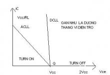
where will Q AC point lie ?
Maybe a slight paraphrasing will help or maybe it won't, here's how I look at it. At DC instead of considering them push/pull, consider them as 2 CCS tuned to exactly the same current. Then you can treat each one through super positioning and consider for 1/2 the cycle you are varying the current through the top transistor and through the other half you are varying the current through the bottom transistor. Basically it's a PNP and NPN, CCS loaded, EF super positioned on top of eachother.
To find the Q point, try evaluating each PNP/NPN stage independantly and then see what you get.
--
Danny
Latest version
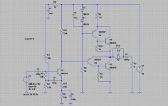
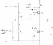
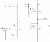
I have been puttering around with this thing a little bit and I am almost to the point where I am ready to start burning some solder. Here is the current version of the schematic.
I am running about 1.5A through the output stage and about 6.5mA through the VAS. I have not settled on values for the caps or R3 yet but the values shown seem to sim alright. I think I have C4 wrong. It is supposed to bypass noise in the diodes so I think it should go to ground instead of V+.
Attachments
You are a predictor.Maybe a slight paraphrasing will help or maybe it won't
 I don't still know.
When Q1 turns on,Q2 turn off. So where can I see the current soucre?
Re: Latest version
Hi,
May i have a question for you about the schematic?
What is the purpose of R5 and R10 ?
Why you choose 10 ohm for this ?
What is the influence to increase or decrease the resistor value ?
Thank you very much in advance .
ward
mashaffer said:I have been puttering around with this thing a little bit and I am almost to the point where I am ready to start burning some solder. Here is the current version of the schematic.
I am running about 1.5A through the output stage and about 6.5mA through the VAS. I have not settled on values for the caps or R3 yet but the values shown seem to sim alright. I think I have C4 wrong. It is supposed to bypass noise in the diodes so I think it should go to ground instead of V+.
Hi,
May i have a question for you about the schematic?
What is the purpose of R5 and R10 ?
Why you choose 10 ohm for this ?
What is the influence to increase or decrease the resistor value ?
Thank you very much in advance .
ward
Re: Re: Latest version
Hi Ward;
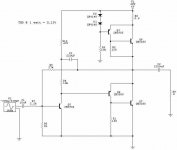
Those were suggested to me by Halojoy. They are used to increase the current in the PNP devices in order to improve linearity. I have not simulated with different values yet. It might be interesting to try but I am not to confident in the distortion figures that I get from the simulations anyway.
ward said:
Hi,
May i have a question for you about the schematic?
What is the purpose of R5 and R10 ?
Why you choose 10 ohm for this ?
What is the influence to increase or decrease the resistor value ?
Thank you very much in advance .
ward
Hi Ward;
Those were suggested to me by Halojoy. They are used to increase the current in the PNP devices in order to improve linearity. I have not simulated with different values yet. It might be interesting to try but I am not to confident in the distortion figures that I get from the simulations anyway.
Hi,
I did not fllow this whole thread, but stept in and looked at your schematic.
I think it might actually work with some adjustments. R5 and R10 as 10 Ohm, isn't that a bit too low. This will cause a current flow of > 65mA in the driver transistors... that cann't be right. Better use something like 100 Ohm therer, and replace the 2N3055 with a darlington tip141 (?) or something like that..
I would re-arange the first stage , the gain stage, with some local feedback from the collector, to lower the output impedance that drives the output stage..
Goodluck, keep us posted,
Regards,
Thijs
tschrama said:Hi,
I did not fllow this whole thread, but stept in and looked at your schematic.
I think it might actually work with some adjustments. R5 and R10 as 10 Ohm, isn't that a bit too low. This will cause a current flow of > 65mA in the driver transistors... that cann't be right. Better use something like 100 Ohm therer, and replace the 2N3055 with a darlington tip141 (?) or something like that..
I would re-arange the first stage , the gain stage, with some local feedback from the collector, to lower the output impedance that drives the output stage..
Goodluck, keep us posted,
Regards,
Thijs
I have thought about collector feedback and may try it. Played with it a little bit in LTspice but did not notice any improvement in fact sometimes it all went to heck when I added the feedback. Possibly I was doing it wrong. I just put a cap and resistor in series from collector to base.
I will probably play with it a little bit once I have the circuit laid out. It is a fairly simple matter to add it but I would also need to vary the open loop gain to compensate. Maybe putting an emitter bypass cap on the wiper of a pot used for the emitter resistor.
Why do you think that 65mA is too much. That is less than 10% of the rated Ic for that device?
I think that a darlington would be redundant given that I am already using the complementary pair output wouldn't it?
 .
.Hi,
Nice to see your reply so soon online..
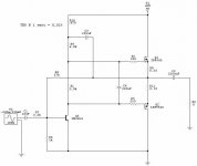
About the feedback: just look at the schematic.. this arangement take care of the bias-point too... 65mA for the drivers is way too much.. look at the power they are dissipation ( I x V !) .. not a good idea.. the 2n3055 have too low current gain ( +/- 60?) .. a couple of tip141 shouldn't cost more that 4 $, but will enable to build a real performing amplifier...
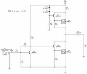
I just went ahead and simulated a 2N3055 version too....
Nice to see your reply so soon online..
About the feedback: just look at the schematic.. this arangement take care of the bias-point too... 65mA for the drivers is way too much.. look at the power they are dissipation ( I x V !) .. not a good idea.. the 2n3055 have too low current gain ( +/- 60?) .. a couple of tip141 shouldn't cost more that 4 $, but will enable to build a real performing amplifier...
I just went ahead and simulated a 2N3055 version too....
Attachments
Re: Re: Re: Latest version
Hi,
Thanks for your reply.
Regarding the resistors,
Does it work as local feedback when AC signal applied,too.
Thanks
ward
mashaffer said:
Hi Ward;
Those were suggested to me by Halojoy. They are used to increase the current in the PNP devices in order to improve linearity. I have not simulated with different values yet. It might be interesting to try but I am not to confident in the distortion figures that I get from the simulations anyway.
Hi,
Thanks for your reply.
Regarding the resistors,
Does it work as local feedback when AC signal applied,too.
Thanks
ward
tschrama said:Hi,
Nice to see your reply so soon online..
About the feedback: just look at the schematic.. this arangement take care of the bias-point too... 65mA for the drivers is way too much.. look at the power they are dissipation ( I x V !) .. not a good idea.. the 2n3055 have too low current gain ( +/- 60?) .. a couple of tip141 shouldn't cost more that 4 $, but will enable to build a real performing amplifier...
I just went ahead and simulated a 2N3055 version too....
Oh, of course! Thanks for pointing that out. When I increased V+ from 15V to 40V I neglected to adjust those resistors! As I look at it I am probably getting plenty of current without R5 and R10 with this higher supply voltage. In fact I think that I will need to use a medium power PNP device instead of the small signal device at this high voltage. I think I like that better than going to a triple gang (i.e. compmentery pair + Darlington) output. Something in a TO-220 case should be fine although the hfe may be somewhat smaller than I calculate below.
The current gain of the complementary pair is about 5000 (min. hfe for 2907 = 50 and hfe for the 2033 is over 100 at 1.5A per data sheets) so I should only be drawing about 300uA from the VAS. Biasing at ten times the current draw is still only 3mA. Am I missing something here also?
From looking at your circuits I think I see where I went wrong on the feedback. You are using DC feedback (kind of like a self bias circuit). I left the voltage divider bias intact and just added a capacitively coupled feedback resistor from collector to base.
One thing that worries me about your circuits though is the apparently low input impedence. I chose voltage divider bootstrap bias to prevent loading of the preamp.
After that... you can easely take the feedback point from the amplifiers output instead of just the gain-stage...
THen I decided to bootstrap the gain stage, giving higher openloop gain, more feedback, less distortion... this one actually performes quite good..
One of the things you missed from earlier in the thread is that one purpose of this project is to specifically investigate what can be done without interstage feedback. So some aspects of your modifications, which no doubt produce very nice performance, run counter to the purpose in this case. So maximizing VAS gain and then adding gobs of GNF is exactly what I am trying to avoid.
I actually considered using a CCS or bootstrap on the VAS for the sake of increased linearity but found that it was difficult to control the gain without GNF which I was trying to avoid. Maybe with your different bias design I could use CCS and local feedback in the VAS. I will have to look into that.
I am enjoying your input. I like the down to the detail analysis. Very challenging.
Sorry... no interest in MOSFETs for anything but current sources and switches. Chalk it up to prejudice.
Overall I am looking for an open and dynamic amplifier. I am not too concerned with THD figures below 1% as long as odd order harmonics don't dominate. If THD exceeds that of typical speakers or is audibly objectionable then I would be concerned. If I do all I can to get the best performance out of each stage and I still don't get good sound out of it I can tighten the belt up a little bit with GNF.
Hi,
Sorry I didn't read the entire thread.. I now get your point. You're right about the input impedance. Bootstraping the input is a neat idea! In my arangement you can easely multipy all resistance values with 5x or 10x and re-adjust for mid-point voltage 20V... I actualy think you can leave those resistors out at the output pair.. the 2N3055 draws about 15-25mA basecurrent as it is.. this all has to be controlled by the little drivers... maybe indeed use a medium power transy there...
regards,
Thijs
Attachments
- Status
- This old topic is closed. If you want to reopen this topic, contact a moderator using the "Report Post" button.
- Home
- Amplifiers
- Solid State
- New guy on the block thinking class A