Re: Thanks for the tip Danny
I think You have to change the whole topolgy. In Your amplifier the VAS stage has very low output. You can apply other type output stage, with voltage gain, and some feedback, as well.
sajti
mashaffer said:I did as you suggested and googled around a bit. It looks like the load resistor would need to be on the emitter of the first transistor in the pair (I was trying to put it on the emitter of the last transistor).
So are we talking about something like this? The attached file is my stab at a Sziklai output. If I understand it right hFE of the pair is hFEq1 X hFEq2 so that Q1 could be a small signal device and only Q2 would actually pull large current.
Does that look like a workable design? I am not entirely sure about the stability of the bias currents.
I think You have to change the whole topolgy. In Your amplifier the VAS stage has very low output. You can apply other type output stage, with voltage gain, and some feedback, as well.
sajti
sajti said:
Try to add some small resistor between the emitter of the 2N3055, and the ground. It will set some local feedback, and increase the linearity.
sajti
I am not sure. the amp has a compounded pair configuration in the output stage and the "emitter" resistor for the pair is the 7.5ohm resistor sitting on the collector of 2n3055.
adding an emitter resistor to the 2n3055 may limited the voltage swing and adding distortion.
from Millwood:
Are you talking about changes in the value of the top resistor in the voltage divider bias network? I am also planning to try running higher current in the bias network and using a bootstrap resistor to raise the input impedence.
from Sajti:
Possibly. I also have some options for increasing the gain of the VAS stage. My plan is to try to get the best performance I can before adding interstage NFB and then add only what is necessary. I also plan to look at bootstrapping Rcq1 as well as current source or cascode on Q1.
That sounds like a good idea. I imagine that a fractional ohm power resistor would be about right.
As always all input is appreciated. I will look at that other sim software as well. It never hurts to have more than one similar tool on hand.
And distortion is very sensitive to the bias of the first stage: a couple of kohm out and you will immediately see distortion.
Are you talking about changes in the value of the top resistor in the voltage divider bias network? I am also planning to try running higher current in the bias network and using a bootstrap resistor to raise the input impedence.
from Sajti:
I think You have to change the whole topolgy. In Your amplifier the VAS stage has very low output. You can apply other type output stage, with voltage gain, and some feedback, as well.
Possibly. I also have some options for increasing the gain of the VAS stage. My plan is to try to get the best performance I can before adding interstage NFB and then add only what is necessary. I also plan to look at bootstrapping Rcq1 as well as current source or cascode on Q1.
Try to add some small resistor between the emitter of the 2N3055, and the ground. It will set some local feedback, and increase the linearity.
That sounds like a good idea. I imagine that a fractional ohm power resistor would be about right.
As always all input is appreciated. I will look at that other sim software as well. It never hurts to have more than one similar tool on hand.
millwood said:
I am not sure. the amp has a compounded pair configuration in the output stage and the "emitter" resistor for the pair is the 7.5ohm resistor sitting on the collector of 2n3055.
adding an emitter resistor to the 2n3055 may limited the voltage swing and adding distortion.
You have right. Sorry. This was my mistake....
sajti
Simulation
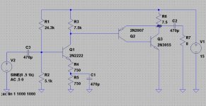
I was able to get LTspice working first so I did some sims with it. Using the circuit attached I got the DC operating point sorted out and ran a transient response on which I did an FFT (it took quite a while for me to figure out that this was the way to do it).
On the next two posts I will attach the resulting FFT and THD calculations.
Attachments
THD Spreadsheet
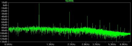
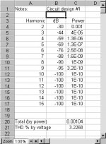
I downloaded a spreadsheet from the net which is supposed to calculate THD from the dB output of an FFT. The results are attached. This shows a bit over 3%. This is about what one would expect but is about 1/2 of what Millwood got so I am suspicious that I have done something wrong.
The interesting thing is that I tried using various layouts including GNFB, NFB around VAS only, Current source load for VAS, Cascode on VAS and standard darlington output. In no case was the distortion reduced by more than about 1% (NFB) and whenever HD2 was reduced (max 3dB) HD3 actually increased.
Got to do some more thinkin'.
Attachments

the fft calculation in ltspice (and others I guess) seems to be quite sensitive to how long you let the simulation run, and windowing. You may want to let it run a little bit longer (I did 100ms and got something that looks different from yours).
I also used perfect transistors (too lazy to use real ones).
Anyway, it should be directionally accurate but not exactly accurate. so take it with a grain of salt.
I also used perfect transistors (too lazy to use real ones).
Anyway, it should be directionally accurate but not exactly accurate. so take it with a grain of salt.
Nelson Pass and Mashaffer
Mr. Nelson.... the one and only is too much lonely, sorry if i capture the damn destiny of the special people that have more knowledge than a most of us.... lonely is an unavoided consequence...if wrong, better...if rigth... sorry to remember you that.
Mr. Mashaffer, i know how you can have Multisim 2001 free.
write directly to me:
nanabrother@yahoo.com
regards,
Carlos
An interesting result
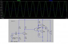
One rather interesting result of the sims is that the lowest distortion (according to the FFT) occured when there was slight clipping (either by overdriving or by feeding the output signal back to the base of the input trans through a cap and very small resistor) of the pos. side of the waveform.
Thanks for the offer Carlos. At the moment I have my hands full with the two that I have. I may shoot you an email later.
P.S.
BTW I didn't mean to ignore Mr. Pass' wise counsel. I appreciate that reminder. After all we don't listen to curves on a computer screen. We listen to real circuits.
As an unemployed former truck driver I am trying to get as good a handle on things as I can before commiting it to hardware.
The next thing I plan to look at is multiple output devices in the form of active loads and push pull class A. I am a little bit concerned about odd order harmonics in a push pull so I will try the active load circuits first. If the potential improvement is high enough I might even spring for the extra buck and a half for another power transistor.
More complex
This circuit uses a simple current mirror to load the output transistor which increased the possible power output significantly. I show the diode version since I have lots of those on hand. It seems like one would not gain any advantage in using a transistor instead of the diode unless it was also a 2N3055. Is that an accurate statement or would it be worthwhile to use a small signal transistor instead of the diode?
Thanks to Henry Johnson for the idea of using the collector resistor on Q2 to increase the quescient current through Q2. You will also note that the current through Q1 has been increased and the emitter bypass capacitor has been removed. As the circuit stands there is enough gain to drive the output just shy of clipping with 1.3v p-p input. If slightly greater sensitivity is needed I think that Q1 can be biased for slightly more gain without any difficulty.
Attachments
So pass me the dunce cap
I must have taken my dumb pills today. I was in the shower when it hit me. Take a look at that "current source". The resistor which is supposed to set the current is modulated with the output signal. 
I think what I need to do is change the transistor to a PNP device with the emitter connected to V+. The diode would then be connected to the V+ also and the current set resistor should run from the diode to ground.
I think that should work.
I must have taken my dumb pills today. I was in the shower when it hit me. Take a look at that "current source". The resistor which is supposed to set the current is modulated with the output signal. I think what I need to do is change the transistor to a PNP device with the emitter connected to V+. The diode would then be connected to the V+ also and the current set resistor should run from the diode to ground.
I think that should work.
Re: So pass me the dunce cap
a npn current source like yours can work, with some modifications. Take a look at some of nelson's work: he had used n-channel mosfets as current source. i also simulated a similar design but didn't have much success due to thermal run-away. But it can be made to work.
mashaffer said:
a npn current source like yours can work, with some modifications. Take a look at some of nelson's work: he had used n-channel mosfets as current source. i also simulated a similar design but didn't have much success due to thermal run-away. But it can be made to work.
Latest Version
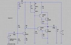
Many, many thanks to Halojoy who has been very helpful with the current source as well as other circuit details!
The attached jpeg is the current state of the design project. I have been toying with the idea of using choke loading instead of the CCS but I suspect that I will end up with something very close to this CCS design.
The simulation indicates that this circuit should give frequency response that is 3dB down at about 17Hz and 200kHz. If I remember right the power output was more than 6 watts. If I actually get that kind of results I will be very pleased.
Of course the PS shown is an ideal voltage source and using a real PS will effect the results. I may go ahead and simulate the actual PS as well but right now I intend to use an exiting 15V 1.6A PS that was salvaged from who knows what. I will put additional RC filtering on the amplifier board.
The circuit diagram shows all fixed resistors for the purposes of the simulation. Obviously the bias and current adjust resistors would have to include an adjustable portion. Also note that not all of the devices shown are the actual devices that will be used because I don't have models for all of the devices that I intend to use. Therefore some values may be somewhat different.
The values shown result in about 1 Amp through the 3055s.
Attachments
You may have a point but...
a big part of the reason for this design project is educational. I wanted to see what I could do with a relatively simple design without interstage NFB. I could later add some feedback and hear the difference directly. The main point is the learning experience.
BTW it occured to me that since I will need to buy another power transistor and since only one of them will be used to amplify the signal while the other is a current source they would not need to be the same type would they? I could then select a newer transistor with better performance and use the 3055 as the current source.
Does anyone have any suggestions (within reasonable price range)? I would be insterested in your opinions as the the best output transistor for this application and why?
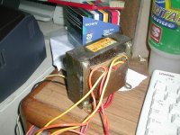
I also discovered that I have a huge power transformer lying around which will allow me to go with a 30V - 40V power supply. At first I thought it was for tubes because of the size and plethora of secondary taps (see attached pic). However, I put 12V ac across the primaries and all of the outputs measured between 1.5V and 4V (don't remember exact figures). I figure that I can make a mongo power supply out of it and use it for this project and add other pieces gradually to come up with a transitor multi amp system.
Eventually I want to do the same thing in tubes. My thoughts are to have triamping plus subwoofer. Maybe low power SE Class A for tweeters , higher power SE Class A for midrange, matbe push-pull Class A for midbass and either push-pull Class A or AB for subwoofer.
If I manage to get some good horns going I might not need to use AB at all.
a big part of the reason for this design project is educational. I wanted to see what I could do with a relatively simple design without interstage NFB. I could later add some feedback and hear the difference directly. The main point is the learning experience.
BTW it occured to me that since I will need to buy another power transistor and since only one of them will be used to amplify the signal while the other is a current source they would not need to be the same type would they? I could then select a newer transistor with better performance and use the 3055 as the current source.
Does anyone have any suggestions (within reasonable price range)? I would be insterested in your opinions as the the best output transistor for this application and why?
I also discovered that I have a huge power transformer lying around which will allow me to go with a 30V - 40V power supply. At first I thought it was for tubes because of the size and plethora of secondary taps (see attached pic). However, I put 12V ac across the primaries and all of the outputs measured between 1.5V and 4V (don't remember exact figures). I figure that I can make a mongo power supply out of it and use it for this project and add other pieces gradually to come up with a transitor multi amp system.
Eventually I want to do the same thing in tubes. My thoughts are to have triamping plus subwoofer. Maybe low power SE Class A for tweeters , higher power SE Class A for midrange, matbe push-pull Class A for midbass and either push-pull Class A or AB for subwoofer.
If I manage to get some good horns going I might not need to use AB at all.
Attachments
- Status
- This old topic is closed. If you want to reopen this topic, contact a moderator using the "Report Post" button.
- Home
- Amplifiers
- Solid State
- New guy on the block thinking class A