Hi,
This kit is a much better choice than the Analogmetric stuff. It has a certain degree of originality.
Analogmetric stuff through the bank are badly executed, unauthorised copies of "famous" (not necessarily good, just famous) stuff...
Ciao T
I have just bought a Nos/Os dual tda1541a (parallel) kit from rainbow_hui on ebay.
It uses a WM8805 & 26c32 front end, + SAA7220 which can be bypassed with a couple of jumpers and has onboard psus. (discrete)
This kit is a much better choice than the Analogmetric stuff. It has a certain degree of originality.
Analogmetric stuff through the bank are badly executed, unauthorised copies of "famous" (not necessarily good, just famous) stuff...
Ciao T
Thorsten, I wonder if you have heard the analogmetric board?
Though, compared to your modified satch or AMR, perhaps it would sound like garbage? LOL I guess it depends what you are used to?
I have the raindrop hui board as well, and another one.
AFAIC, the analogmetric is pretty good, there are limitations to the PCB layout, some glaring errors, (and wrong theory like asynchronous reclocking) and if I were to do my own board, it would be different to all of the above, however, after DEM reclocking you can still get a pretty decent sound out of this board, which still "beats" (for want of providing a long winded review) all delta sigma DACs I have heard, so IMO people with this board should not be discouraged. At least with the analogmetric you can just buy the PCB for a paltry $25. All the other available "kits" involve a lot more cost, so for those on a budget, the analogmetric is a good choice, provided you can buy the other parts at a good cheap price.I built mine for about $100 which I thought was good.
IMO those seeking the "best" sounding kit should save up a bit longer and choose one of the other options available, preferably one with a valve output stage. Or design your own board.
Last edited:
Hi,
No, but ones based on the same design.
This whole thing basically is faulty by design and requires removal of the idiotic async reclocking to be even considered functional.
If you are going to be building something completely different, that is okay, if you know what you are doing. To build it as kit is useless.
Given the layout I have seen over at Luksz's site they layout is not terrible, it is not even that good. The layout for the decoupling cap's is even more incompetent than most I have seen.
Honestly, if you know enough to make this joke work properly, you can do better using veroboard and copperfoil.
HOW MUCH!? Good Gort, you can get probably get a custom run of 50pcs made for that money in the PRC and that is using top grade materials.
And people keep telling me High End audio is a rip-off...
Veroboard and copper foil for the grounds and a good 3-dimensional layout with the DEM decoupling caps below the TDA1541, analogue plane with copper foil below the pcb, digital plane above will do miles better...
Ciao T
Thorsten, I wonder if you have heard the analogmetric board?
No, but ones based on the same design.
This whole thing basically is faulty by design and requires removal of the idiotic async reclocking to be even considered functional.
If you are going to be building something completely different, that is okay, if you know what you are doing. To build it as kit is useless.
Given the layout I have seen over at Luksz's site they layout is not terrible, it is not even that good. The layout for the decoupling cap's is even more incompetent than most I have seen.
Honestly, if you know enough to make this joke work properly, you can do better using veroboard and copperfoil.
At least with the analogmetric you can just buy the PCB for a paltry $25.
HOW MUCH!? Good Gort, you can get probably get a custom run of 50pcs made for that money in the PRC and that is using top grade materials.
And people keep telling me High End audio is a rip-off...
Veroboard and copper foil for the grounds and a good 3-dimensional layout with the DEM decoupling caps below the TDA1541, analogue plane with copper foil below the pcb, digital plane above will do miles better...
Ciao T
you can get probably get a custom run of 50pcs made for that money in the PRC and that is using top grade materials.
Ciao T
Got a manufacturer you recommend?
Hi,
This kit is a much better choice than the Analogmetric stuff. It has a certain degree of originality.
Analogmetric stuff through the bank are badly executed, unauthorised copies of "famous" (not necessarily good, just famous) stuff...
Ciao T
Thanks, that is reassuring.
I had my doubts about AM when they cannot even get the schematic correct - doesn't exactly inspire confidence.
Hi,
Any decent PCB manufacturer that you can find in the PRC (People's Republic of China), no specific recommendation. Most will probably have a 50 to 100USD minimum, so you would have to organise a group buy...
Ciao T
Got a manufacturer you recommend?
Any decent PCB manufacturer that you can find in the PRC (People's Republic of China), no specific recommendation. Most will probably have a 50 to 100USD minimum, so you would have to organise a group buy...
Ciao T
This is just what I wanted !
You may regret this offer - coz I've got loads of questions
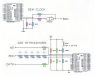
I have found a 74HCUO4N, the quad 74HC175N in my scrap box and have the resistors to do DEM now.
EC designs and Thorsten think it's ok to use a 2.8 mhz clock signal ( via resistors of course ) to pins 16 and 17 - this is what I want to do in the next hour.....( ok... I'll wait until the sun comes up at your side )
On the 74HCU04 pin 7 is gnd, 14 is v+ and pins 1 and 2 are both receiving
' something ' ( haha ) from the -15 volt rail via the 3.3 resistors and then both these pins ( 1 & 2 ) re distribute to pins 16 and 17 via the 10k resistors. Where do I feed in my raw 2.8 mhz clock signal ?
I'm lashing something together p2p as we speak on vero board to see how it will all go together ( i'll post a pic soon of this ) I don't want to hear any laughter either !!
I like the idea of a 7805 ps for it too - so any advice on this would be good. Have some half decent + 5v basic teddy regs I can use that I made a while back which can easily accommodate the 15 ma of current the inverter draws at 5 volts.
I understand that if a resistor is connected to the input and output the inverter will bias itself into a linear state and the input and output pins will settle into a voltage of half the incoming rail voltage....
There's my confusion - will it run at 2.5 volts or have I misunderstood something here ?
Also, I read that all unused input pins must be connected to ground or the +ve rail - the unused inverters then draw o or virtually no current at all. Any need to do this in the context of the application ?
That's it for one day -I'll post a pic of this p2p ' thing ' up soon
Andrew
NO LAUGHING
Andrew,
Reclocking using a 74HC04 does this:
Bass becomes tighter and conveys tone better, leading edges of notes are faster and more defined, High frequenices loose the slight fuzzyness and become crystal clear. High hats sound like real high hats, brassy and fast. Overall detail improves vastly over the stock sound using the cap. Background sounds and "atmosphere" are easilly heard. The prominent midrange sound of the TDA1541 goes away. The sound is more balanced from top to bottom. Bass goes deeper and more realistic. highs seem to go higher and cleaner. There is NO downside whatsoever. Like I said earlier, everything gets better
Is "advanced reclocking" the same as asyncronously reclocking? I thought that was no good becuse you are dropping the odd sample because the separate clock is not syncronised to the incoming SPDIF signal.
Or are you talking about a CD player?
It's an old Arcam Alpha and what I mean by advanced clocking is :
11.289 to 7220
11.289 to 7310
5.6 and 11.289 to pins 2 and 4 of TDA1541 -
I was sure ecdesigns has referred this to this arrangement as advanced.
The above is generated by ONE clock with dividers @ 11.2 - 5.6 - 2.8
On my other DAC I just used a 7805 chip feeding the 74HC04, point to point wiring, nothing particularly neat or nice looking, but it works like a charm.
any more questions, let me know.
You may regret this offer - coz I've got loads of questions
I have found a 74HCUO4N, the quad 74HC175N in my scrap box and have the resistors to do DEM now.
EC designs and Thorsten think it's ok to use a 2.8 mhz clock signal ( via resistors of course ) to pins 16 and 17 - this is what I want to do in the next hour.....( ok... I'll wait until the sun comes up at your side )
On the 74HCU04 pin 7 is gnd, 14 is v+ and pins 1 and 2 are both receiving
' something ' ( haha ) from the -15 volt rail via the 3.3 resistors and then both these pins ( 1 & 2 ) re distribute to pins 16 and 17 via the 10k resistors. Where do I feed in my raw 2.8 mhz clock signal ?
I'm lashing something together p2p as we speak on vero board to see how it will all go together ( i'll post a pic soon of this ) I don't want to hear any laughter either
!!I like the idea of a 7805 ps for it too - so any advice on this would be good. Have some half decent + 5v basic teddy regs I can use that I made a while back which can easily accommodate the 15 ma of current the inverter draws at 5 volts.
I understand that if a resistor is connected to the input and output the inverter will bias itself into a linear state and the input and output pins will settle into a voltage of half the incoming rail voltage....
There's my confusion - will it run at 2.5 volts or have I misunderstood something here ?
Also, I read that all unused input pins must be connected to ground or the +ve rail - the unused inverters then draw o or virtually no current at all. Any need to do this in the context of the application ?
That's it for one day -I'll post a pic of this p2p ' thing ' up soon
Andrew
NO LAUGHING
Hi,
I think we may have various confusions for the various types of reclocking (and other mods) with the TDA1541 circuits.
1) Asynchronous reclocking of the data to the DAC Type A (monumentally stoopeed, makes Wiley E. Coyote look a Genius)
This is commonly done in these kits etc. by supplying a clock to the CS8412/CS8414. The problem with is that if a sample is dropped or repeated the result is a small click, like surface noise from the LP.
This can be quite small IF you purchase a super accurate (1ppm guaranteed clock deviation) clock for both your transport and dac, the result is one such click every halve million samples, or every 11 seconds in the worst case.
With a lot of music these clicks are not obvious, but with Solo Piano for example they are annoying. And if you have a greater range of differences between the clocks the clicks are more frequent and more annoying. With a not uncommon difference of 200ppm between the clocks then we get around 10 clicks per second.
And of course, if using a source that handles multiple sample rates only one is usable at all. This actually applies to ALL DAC's that use this, not just TDA1541 based.
2) Asynchronous reclocking of the data to the DAC Type B (not so stupid, but unpredictable)
This is done by reclocking the signal into the DAC with Flip Flops that are fed a very high frequency that is completely unrelated to the sample rate, the higher is better, 125MHz seems a sensible limit for DIY.
To the best I know it originated with Kusonoki San (who also started the revival of non-oversampling DAC's - all early Japanese CD-Players where Non-Oversampling of course).
This reclocking will reliably cause cyclic jitter of a peak to peak value equal to the period of the clock. The jitter frequency components will be essentially multiplied and aliased to higher frequencies. This can successfully alias a lot of the audio band jitter to frequencies above, which in multibit DAC's means they become a much reduced problem. This does not work for Delta Sigma DAC's of course.
There is no link to the sample rate so this works with all sample rates. However the operation of this system is somewhat unpredictable, as we essentially rely on "beat" products, so we may end up making previously inaudible very low frequency jitter audible, by aliasing them into the audible range.
3) TDA1541 Dynamic Element Matching reclocking
This synchronises the DEM oscillator with a multiple of the word clock and in the process makes sure that each sample uses all Elements in the system (minimum error for each sample) and ideally uses multiple cycles of dynamic matching for each sample.
This was first mentioned here on DIYA by Henk Ten Pietrik (sorry if I get the name wrong), but as we have seen in other threads it was also on previous occasions used by for example Grundig.
4) TDA1541 I2S Signal Attenuation
This is not re-clocking as such, it has been discussed here before. The TDA1541, while specified for TTL signals on the input, actually internally uses a kind of non-standard emitter coupled logic. TTL signals actually overdrive the input stage and cause all sorts of interesting results.
By attenuating the signal levels the problems are reduced, if we can precisely match the swing required by the TDA1541 AND compensate the quite substantial thermal drift of the TDA1541's logic (yes, I do know how to do that, it is not doable DIY style I'm afraid).
The solutions shown by ECdesigns are much easier and can be done DIY style.
5) Asynchronous Sample Rate Converters
This again is not re-clocking as such. It does however allow the DAC chip to be supplied by a local clock. This can be important for Delta Sigma based DAC's who have normally an appalling level of sensitivity to jitter on the system clock.
Due to the nature of the asynchronous conversion, the process cannot avoid being lossy and there are other issues (jitter is not really removed, but aliased into other domains), however with DS DAC's that have severe system clock sensitivity the end-result may still be preferable to avoiding the drawbacks of ASRC (of course, the Technocrats believe fervently there are no drawbacks).
I hope this overview clarifies where things stand, at least the way I see it.
YMMV.
Ciao T
This is just what I wanted !
I think we may have various confusions for the various types of reclocking (and other mods) with the TDA1541 circuits.
1) Asynchronous reclocking of the data to the DAC Type A (monumentally stoopeed, makes Wiley E. Coyote look a Genius)
This is commonly done in these kits etc. by supplying a clock to the CS8412/CS8414. The problem with is that if a sample is dropped or repeated the result is a small click, like surface noise from the LP.
This can be quite small IF you purchase a super accurate (1ppm guaranteed clock deviation) clock for both your transport and dac, the result is one such click every halve million samples, or every 11 seconds in the worst case.
With a lot of music these clicks are not obvious, but with Solo Piano for example they are annoying. And if you have a greater range of differences between the clocks the clicks are more frequent and more annoying. With a not uncommon difference of 200ppm between the clocks then we get around 10 clicks per second.
And of course, if using a source that handles multiple sample rates only one is usable at all. This actually applies to ALL DAC's that use this, not just TDA1541 based.
2) Asynchronous reclocking of the data to the DAC Type B (not so stupid, but unpredictable)
This is done by reclocking the signal into the DAC with Flip Flops that are fed a very high frequency that is completely unrelated to the sample rate, the higher is better, 125MHz seems a sensible limit for DIY.
To the best I know it originated with Kusonoki San (who also started the revival of non-oversampling DAC's - all early Japanese CD-Players where Non-Oversampling of course).
This reclocking will reliably cause cyclic jitter of a peak to peak value equal to the period of the clock. The jitter frequency components will be essentially multiplied and aliased to higher frequencies. This can successfully alias a lot of the audio band jitter to frequencies above, which in multibit DAC's means they become a much reduced problem. This does not work for Delta Sigma DAC's of course.
There is no link to the sample rate so this works with all sample rates. However the operation of this system is somewhat unpredictable, as we essentially rely on "beat" products, so we may end up making previously inaudible very low frequency jitter audible, by aliasing them into the audible range.
3) TDA1541 Dynamic Element Matching reclocking
This synchronises the DEM oscillator with a multiple of the word clock and in the process makes sure that each sample uses all Elements in the system (minimum error for each sample) and ideally uses multiple cycles of dynamic matching for each sample.
This was first mentioned here on DIYA by Henk Ten Pietrik (sorry if I get the name wrong), but as we have seen in other threads it was also on previous occasions used by for example Grundig.
4) TDA1541 I2S Signal Attenuation
This is not re-clocking as such, it has been discussed here before. The TDA1541, while specified for TTL signals on the input, actually internally uses a kind of non-standard emitter coupled logic. TTL signals actually overdrive the input stage and cause all sorts of interesting results.
By attenuating the signal levels the problems are reduced, if we can precisely match the swing required by the TDA1541 AND compensate the quite substantial thermal drift of the TDA1541's logic (yes, I do know how to do that, it is not doable DIY style I'm afraid).
The solutions shown by ECdesigns are much easier and can be done DIY style.
5) Asynchronous Sample Rate Converters
This again is not re-clocking as such. It does however allow the DAC chip to be supplied by a local clock. This can be important for Delta Sigma based DAC's who have normally an appalling level of sensitivity to jitter on the system clock.
Due to the nature of the asynchronous conversion, the process cannot avoid being lossy and there are other issues (jitter is not really removed, but aliased into other domains), however with DS DAC's that have severe system clock sensitivity the end-result may still be preferable to avoiding the drawbacks of ASRC (of course, the Technocrats believe fervently there are no drawbacks).
I hope this overview clarifies where things stand, at least the way I see it.
YMMV.
Ciao T
Thorsten Hi
Thanks for the very detailed and lengthy reply and.... your patience.
I'm now not sure at all what clocking method I've got and maybe it's not so important if I can get the DEM part right.
So I just found a 74HCU04 to do the job and am keen to complete and install it.
This is ow my machine is right now :
Arcam Alpha :
11.289 clock feed to SAA7220
11.289 clock feed to SAA7310
and 5.6 and 11.289 to pins 2 and 4 of TDA1541 - It works well and sounds better than it did - so it should too.
I was sure ecdesigns has referred this to this arrangement as advanced.
The above is generated by ONE clock with dividers @ 11.2 - 5.6 - 2.8
The spare 2.8 is what I want to use on pins 16 and 17 - as I've told you already - sorry if it's getting repetitive.
I just need to know where to feed my 2.8 mhz clock signal from the master clock into the 74HCU04 as Erin showed in his attachment.
Many thanks
Andrew
Erin Hi
Must I do the i2s attenuators too or can I just do the other one ( 74HC04 ) and leave the clocking arrangement I have as it is ?
What do you think of the other arrangement - I'm sure ecdesigns suggested this one too.
Thanks
Andrew
Must I do the i2s attenuators too or can I just do the other one ( 74HC04 ) and leave the clocking arrangement I have as it is ?
What do you think of the other arrangement - I'm sure ecdesigns suggested this one too.
Thanks
Andrew
Attachments
Erin Hi
Must I do the i2s attenuators too or can I just do the other one ( 74HC04 ) and leave the clocking arrangement I have as it is ?
What do you think of the other arrangement - I'm sure ecdesigns suggested this one too.
Thanks
Andrew
You do not have to do the i2s attenuators. But as Thorsten wrote earlier, there are advantages in using them to avoid overdriving the input circuit of this chip. I have no doubt that i2s will yeild an improvement. I have not tried it yet, but I will when I feel motivated to do so. But DEM reclocking will give a tremendous improvement on its own.
I think the other arragement is the Grundig way of doing it that Thorsten mentioned just before. I can only go off what I have read, if im wrong, im sure someone will correct me. The EC designs version uses the -15V bias to saturate the oscillator circuit in the chip to prevent random oscillations, yet still allow the bit clock to drive the oscilator. EC designs circuit seems to be popular at the moment. I'm sure the Grundig version must also be reliable for them to use it in a commercial product. Perhaps you can try both?
Last edited:
Hi,
As you use a CD-Player you have a local clock, which eliminates the need for async reclocking etc.
The old Philips based CD-Players often have a lot of PSU noise which will worsen their jitter though, it is important to clean things up as much as possible (chokes, ferrite beads etc, SMD ceramic caps and Sanyo Os Cons).
Go for it. You may also want to try adding teh I2S Ateenuators as shown in the design by ecdesigns erin attached. Incidentally I am using this exact circuit on my modified Satch. It is simple and gets a big improvement for such a small effort.
While you can use 2.822MHz for DEM reclock, with the kind of layout in the machines of the time I doubt this will be optimum. Try 2.822MHz divided by four or eight instead...
Ciao T
I'm now not sure at all what clocking method I've got
As you use a CD-Player you have a local clock, which eliminates the need for async reclocking etc.
The old Philips based CD-Players often have a lot of PSU noise which will worsen their jitter though, it is important to clean things up as much as possible (chokes, ferrite beads etc, SMD ceramic caps and Sanyo Os Cons).
and maybe it's not so important if I can get the DEM part right. So I just found a 74HCU04 to do the job and am keen to complete and install it.
Go for it. You may also want to try adding teh I2S Ateenuators as shown in the design by ecdesigns erin attached. Incidentally I am using this exact circuit on my modified Satch. It is simple and gets a big improvement for such a small effort.
The spare 2.8 is what I want to use on pins 16 and 17 - as I've told you already - sorry if it's getting repetitive.
I just need to know where to feed my 2.8 mhz clock signal from the master clock into the 74HCU04 as Erin showed in his attachment.
While you can use 2.822MHz for DEM reclock, with the kind of layout in the machines of the time I doubt this will be optimum. Try 2.822MHz divided by four or eight instead...
Ciao T
Thorsten Hi
I just need to know where to feed my 2.8 mhz clock signal from the master clock into the 74HCU04 as Erin showed in his attachment.
Many thanks
Andrew
Where its labelled BCK (bit clock) on his schematic!
The datasheet shows the dem clock range using the internal oscillator to be 200khZ so maybe Thorsten's suggestion to divide bck by 4 or 8 would be worth trying. (using a 74HC4040 again)
Hi,
You use it to divide the BCK to WCK * 4 and then use the grundig circuit posted here....
Ciao T
How could I do the DEM re-clocking with the 74HC4020?
You use it to divide the BCK to WCK * 4 and then use the grundig circuit posted here....
Ciao T
OK, one 2.8 mhz signal into bck - it may be obvious to you guys !!!
The divide by 4 or 8 - how do I do that ? Should I try it without first and see what happens ?
Apologies for this too if it's a daft question - does the 74HCU04 do the divide by 4 and 8 ? too ?
On the diagram ( this might just be the last question )....do I bridge pins 2 and 3 with a wire link - like 2 and 3 are connected to receive BCK ?
I think that's it
Thanks
Andrew
You do not have to do the i2s attenuators. But as Thorsten wrote earlier, there are advantages in using them to avoid overdriving the input circuit of this chip. I have no doubt that i2s will yeild an improvement. I have not tried it yet, but I will when I feel motivated to do so. But DEM reclocking will give a tremendous improvement on its own.
I think the other arragement is the Grundig way of doing it that Thorsten mentioned just before. I can only go off what I have read, if im wrong, im sure someone will correct me. The EC designs version uses the -15V bias to saturate the oscillator circuit in the chip to prevent random oscillations, yet still allow the bit clock to drive the oscilator. EC designs circuit seems to be popular at the moment. I'm sure the Grundig version must also be reliable for them to use it in a commercial product. Perhaps you can try both?
Many thanks - actually it looks a lot easier than using the D flip flop but I will try both.
Are they 1 uf caps by any chance and which diode value is required - can't be much - any diode OK ? 1N400....
Andrew
Hi,
You use it to divide the BCK to WCK * 4 and then use the grundig circuit posted here....
Ciao T
This seems very complicated to me can you draw it out please.
Hi,
Not really.
BCK is the bitclock. It relates to a number of parameters.
For 16/44.1 four time oversampling BCK MUST BE 5.6448MHz.
That is of course BCK to the DAC, not the clock to the DEM reclocker.
Well, I guess you can. The problem is you are largely working blind, not just in the sense of quantifying, but in the sense of understanding how it works. It is not a good place for experimentation.
No, it does not (as one look at the datasheet confirms).
Okay, within reason consider the schematics by ECdesigns, Grundig or me as concepts. They need to be understood and applied. Using then 1:1 only works well if "all else" (your PCB layout, your parts etc.) match what we use. If you do not do that, they need to be interpreted and adjusted.
So to ask "where do I put the 2.8MHz is not helping you, even if you get an answer.
Ciao T
OK, one 2.8 mhz signal into bck - it may be obvious to you guys !!!
Not really.
BCK is the bitclock. It relates to a number of parameters.
For 16/44.1 four time oversampling BCK MUST BE 5.6448MHz.
That is of course BCK to the DAC, not the clock to the DEM reclocker.
The divide by 4 or 8 - how do I do that ? Should I try it without first and see what happens ?
Well, I guess you can. The problem is you are largely working blind, not just in the sense of quantifying, but in the sense of understanding how it works. It is not a good place for experimentation.
Apologies for this too if it's a daft question - does the 74HCU04 do the divide by 4 and 8 ? too ?
No, it does not (as one look at the datasheet confirms).
On the diagram ( this might just be the last question )....do I bridge pins 2 and 3 with a wire link - like 2 and 3 are connected to receive BCK ?
Okay, within reason consider the schematics by ECdesigns, Grundig or me as concepts. They need to be understood and applied. Using then 1:1 only works well if "all else" (your PCB layout, your parts etc.) match what we use. If you do not do that, they need to be interpreted and adjusted.
So to ask "where do I put the 2.8MHz is not helping you, even if you get an answer.
Ciao T
- Status
- This old topic is closed. If you want to reopen this topic, contact a moderator using the "Report Post" button.
- Home
- Source & Line
- Digital Source
- Need help with Analogmetric TDA1541 DAC