steenoe said:
I suggested up to 21,5mm for C1, with some smaller options too.
Just checked my local supplier and it seem that a 22uF NP cap is 2,5mm, thats a 35v cap. I would like to see an option for C2 and C3 with two sets of holes, for use with normal electrolytics, if it will not confuse matters. (just point the neg's toward each other) If so 2,0mm leg dist.
Steen.
Edit. Forgot, filmcap bypass for C2 and C3.
Cool
 I have some 33uf BP lytics the same size. I had already planed on the 21.5mm caps for you Steen.
 Cheers!
Russ
Russ White said:So, why don't you guys give me some suggestions for lead spacing for C1 C2 and C3.
Cheers!
Russ
Let’s see if we get some input from others.
But for the time being I would keep the the 5 mm spacing for C3. A good choice would be a BG NP, second choice Panasonic FC.
Now coming to the output cap C2. It has been a custom for most of us to use the best polyprop (MKP) one can deal with in this position. Space should allow at least for a 10uf Solen brand cap.
Not so sure for what to do with the input cap C1, if needed. I’ll have a look at what was the input impedance of the NS10 was. The input cap will be needed only for sources without an output cap. All of this refers to a double rail NS10.
Ok, I checked the input impedance of the circuit which Threshold (NP) stated at 25K. A 1uf should do then. My take would be a WIMA (MKP again) or similar.
That must be pretty closeWhat do you think?
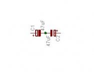
Just to be clear, here is another way to make a non-polar cap. The attached schematic equals approx 22uF NP electrolytic.You dont have to change the board, Russ, I just want to make sure you get the idea, if you didn't allready
Made this way, both options are possible. If you wanted to go with the NP, just jumper one set of pads.Steen.
Edit. Just spotted something. Wouldn't it be possible to connect the two GND tracks from C4 and C5 directly to the GND tracks (the solderpads) of C7 and C6? That would give a bit more distance between the tracks, making it a bit easier to make the boards
Attachments
Hi Steen,
Yes, I knew what you meant about the two polar caps. I have done it before. But there are on the market now quite a few very good non-polars in 2.5 and 5mm. Nichicon Muse comes to mind. Rubycon also has some pretty good ones.
I like to keep my return path to ground seperate as I did, but I would be happy to change it (If I do I will make the path beefier).
The reason for sperate traces to PGND is that the traces have some resistance, and by having multimple caps on the same trace you form a small voltage divider at the cap under a load, which is not really desirable. This is a trick I learned from my firend who does RF circuits, but it works well for audio too. It makes amps less likely to oscillate.
Cheers!
Russ
Oh, I seeThe reason for sperate traces to PGND is that the traces have some resistance, and by having multimple caps on the same trace you form a small voltage divider at the cap under a load, which is not really desirable. This is a trick I learned from my firend who does RF circuits, but it works well for audio too. It makes amps less likely to oscillate.
I suggest you leave them as they are, then Steen
Re: What do you think?
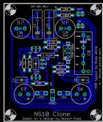
That board is coming up pretty nice Russ.
I see you have kept the NP output cap. Well this is a proto board and we can’t be too picky. But the way we implement it is the way it will sound and will determine if we like it or not.
I love those separate ground traces, especially for input and output connections, makes a nice star ground.
For the film bypass at the rails, and others, is better to connect the film cap directly to the lytic and not on a separate ground trace. The idea here is that both caps, lytic and film bypass, should work as a single unit as seen by the circuit. So the star ground for a bypassed couple should not apply.
Film bypass for the rail lytic could be a bit bigger, say 0.47uf MKP’s if this can be squeezed in.
And this is a tip for when you implement and test the circuit. Using bypass on C2 and C3 will change the balance of the overall sound, generally thinning it. My pick is usually not adding a bypass there, that’s the reason for using the best caps you have at hand for those.
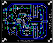
Russ White said:Getting closer to what you want?
That board is coming up pretty nice Russ.
I see you have kept the NP output cap. Well this is a proto board and we can’t be too picky. But the way we implement it is the way it will sound and will determine if we like it or not.
I love those separate ground traces, especially for input and output connections, makes a nice star ground.
For the film bypass at the rails, and others, is better to connect the film cap directly to the lytic and not on a separate ground trace. The idea here is that both caps, lytic and film bypass, should work as a single unit as seen by the circuit. So the star ground for a bypassed couple should not apply.
Film bypass for the rail lytic could be a bit bigger, say 0.47uf MKP’s if this can be squeezed in.
And this is a tip for when you implement and test the circuit. Using bypass on C2 and C3 will change the balance of the overall sound, generally thinning it. My pick is usually not adding a bypass there, that’s the reason for using the best caps you have at hand for those.
Ok since two people I trust say use common trace for the PS bypass caps I will do so.
As for C2 and C3, should I simple make it the same size as C1? Would that be better? Or, as Steen has suggested, are back to back polarized lytics like Panasonic FCs the best option? If so, should they be the 2.5MM sort or the 5mm sort. I would think 25v-50V types would be ok, right?
Cheers!
Russ
As for C2 and C3, should I simple make it the same size as C1? Would that be better? Or, as Steen has suggested, are back to back polarized lytics like Panasonic FCs the best option? If so, should they be the 2.5MM sort or the 5mm sort. I would think 25v-50V types would be ok, right?
Cheers!
Russ
Russ White said:Ok since two people I trust say use common trace for the PS bypass caps I will do so.
As for C2 and C3, should I simple make it the same size as C1? Would that be better? Or, as Steen has suggested, are back to back polarized lytics like Panasonic FCs the best option? If so, should they be the 2.5MM sort or the 5mm sort. I would think 25v-50V types would be ok, right?
Cheers!
Russ
For this proto board i would leave the B2B lytic option since there is always way to install an output polyprop cap which is way bigger than C1. If you would like to fit it on the board you’ll have to increase the size of it since 22.5 mm is too small. I think it’s not wise to do this at this point.
But I must repeat that if someone is using a lytic as output cap there is no need that this be a NP. Just make sure you add some positive bias to the positive terminal of the cap using the pot provided. Using a BP this way is much better than the B2B suggestion.
For the FB cap my pick would be two 47uf Panasonic FC caps on the B2B configuration. A 47uf @ 35V FC cap is 6.3 mm in diameter with 2.5 mm lead separation.
I would suggest to increase the size of the bypass caps at the rails though
apassgear said:
I would suggest to increase the size of the bypass caps at the rails though
To what?
They are current 5mm pitch 13mm diameter. That should be good for 1000uf 50V.
Russ, I think Tony meant C4 and C5To what?
Steen
Edit. 0,47uF MKP was suggested, I think thats a good starting point.
Yep, that would be great. I agree to leaving the outputcap as it is for now. As for the FB cap you might want to add the B2B option with 2,5 mm pin dist. That way you can try both options and hear what sounds bestAh ok, so you thing 5,10,15mm combo pads are good?
Besides that, I wouldnt shy away, doing a proto of the last posted board Steen
Yes, you are right , Choky.-in case of bigger size can be in air- one end on pcb,and other end where it belongs -
Air suspended polyprops
That looks pretty good to meI think I got most of what you said.
Nice job, Russ Steen
choky said:just because I came primary from tube (ptp) world
just my two ounces of vacuum........ hehe
It was just what I did imply. Better explanation, better understanding.
- Status
- This old topic is closed. If you want to reopen this topic, contact a moderator using the "Report Post" button.
- Home
- Amplifiers
- Pass Labs
- My Take on Threshold NS10