
Here is a new, unusual amplifier project: adaptive single-ended class A, feedback-free, error-correcting based on a tringlotron topology, you name it...
It nicely dodges the VFB<->CFB controversy: it doesn't belong to any of the category, being a ZFB type.
ZFB means Zero Feed Back, that is no global feedback.
It relies solely on the error correcting action of the tringlotron to achieve an excellent linearity
The previous project was no-nonsense, maximum bang for buck amp, but this one lavishes in an extravagance of luxury: 13 transistors, and no less than four 2N3055's as output devices!
All of that for a mere 10 ~ 12W per channel.....
Filthy rich....
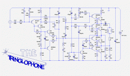
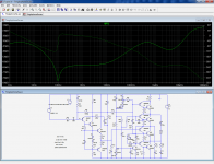
Here is the schematic, details will follow
Attachments
This will send many folk scurrying to Google. Thanks for another great piece of inspiration and work, Elvee.
http://electronicdesign.com/Content/14978/60028_fig.gif
http://electronicdesign.com/Content/14978/60028_fig.gif
the rest of the article on the basic element "tringlotron":
Adding three devices cleverly increases emitter-follower gain
_-_-
(...not like I really understand why it works...)
Adding three devices cleverly increases emitter-follower gain
_-_-
(...not like I really understand why it works...)
Let us look at how the circuit works.
Basically, it comprises two stages: a voltage amplifier having a gain a little greater than 20dB, and a unity gain power buffer.
Let us deal quickly with the VAS: it is the uninteressant part of the circuit (I somewhat had a lack of inspiration at the time).
It is simply a common emitter amplifier based on a CFP (Q12, Q13) for improved linearity.
It is followed by an interstage buffer (Q10, Q11) required to drive the output stage in good conditions.
Nothing particularly smart or original there, the VAS does its job properly, no less, no more.
The output stage:
Now, the interesting bit.
It is a Tringlotron topology, although it isn't apparent at first sight: it looks more like a Quaplotron (quadruplet of P devices in line).
It is actually a Tringlotron, but with some adaptations needed for (relatively) high power operation.
The original, plain vanilla Tringlotron was suitable for low power amplifiers, typically headphones. An example of such an amplifier was the Tringlinator.
But for a larger amplifier, the current and voltage overheads required for proper operation would lead to an excessive power dissipation.
In addition, the Tringlotron is basically a single-ended topology, even if this is not immediately apparent, with the attendant maximal power efficiency limited to 25%.
To deal with the increased power, the single devices have been replaced by CFP's. Since it is desirable to use only N power devices, the resulting composite is of P polarity.
The fourth element (Q1/Q2) is simply a CCS feeding the current into the "Tringle".
But it isn't simply a fixed current, like in a basic Tringlotron: the current is also modulated by the signal through R16/C10.
This improves the efficiency by reducing the tringle standing current, and increasing it when the signal demands it.
Does this change the nature of the single-ended Tringlotron?
Contrary to appearances, no: the Tringlotron correcting mechanism is independent of the standing current: all that is required is that it must be sufficient not to clip the signal.
Unlike a class A push-pull amplifier, the second half contributes in no way to the output power.
This means that this path is purely auxiliary and has no influence on the output signal and its quality: the amplifier remains a true single-ended class A, with its character entirely defined by the Tringlotron.
To be continued....
Here is the schematic, details will follow
great!!!
I was looking for something similar for some time!
the only 2 things are fraighting me:
- why R28/L1 in no feedback amp?
- usinfg cfps... there are the discussions on this forum that it is very oscillating techique...
Clever observation.[*]why R28/L1 in no feedback amp?
The reason is that the Tringlotron synthetizes a ~zero impedance at the speaker terminals.
When it is loaded by a finite impedance, things are just fine.
However, capacitance also presents an impedance --> to zero at an infinite frequency.
And when you try to feed a zero ohm load with a generator also having a zero output resistance, matters go seriously wrong
You are free to use darlingtons instead: the circuit will work almost identically, but with less headroom and a reduced linearity, but nothing really alarming.[*]usinfg cfps... there are the discussions on this forum that it is very oscillating techique...
And such a circuit will certainly be more placid.
Member
Joined 2009
Paid Member
Elvee - very nice work, I really enjoy the line of designs you have put onto the forum, it pushes the thinking beyond the usual and doesn't rely on fancy components. This one is particularly interesting as it lends itself to a hybrid design with a valve based votlage amplifier stage.
as it lends itself to a hybrid design with a valve based votlage amplifier stage.
Bigun
you stole one of my thoughts
")
??? Sorry, I don't see what you meanElvee
did you try correction error input stage like for HP version?
Yes, TIP3055 or MJE3055 would be OK, as any similar transistor.Dear Elvee
I have at about 8 pcs old KD502 but no proper heatsink for them.
Is this possible to use modern TO247s?
If you use faster devices, some corrections might be needed. So far, I only tried 2N3055's.
Pics, in a day or two, PCB nopeplease post some pics, maybe pcb?
Here is one version. Maybe not exactly identical to final graphic schematic, but enough to get you going and have some funalso asc file for tringlophone?
PLEASE!
Thanks, and yes, I think so. For the moment, the VAS does its job, but it is a little... bland shall we say. Alternatives are welcomeElvee - very nice work, I really enjoy the line of designs you have put onto the forum, it pushes the thinking beyond the usual and doesn't rely on fancy components. This one is particularly interesting as it lends itself to a hybrid design with a valve based votlage amplifier stage.
Attachments
Member
Joined 2009
Paid Member
I wouldn't call anything here bland, this CFP input is very nice and perfectly suited to give good linearity, low output impedance and all keeping only local 'current' feedback
Tube input & VAS is fun and easy to do, there are lots of options available to pick from depending on what you want to achieve. You don't need a lot of gain, so a medium-mu tube would be good and if you want lowish impedance from the tube then you could choose a bottle with two triodes and use one as a cathode follower buffer. Lots of options.
Tube input & VAS is fun and easy to do, there are lots of options available to pick from depending on what you want to achieve. You don't need a lot of gain, so a medium-mu tube would be good and if you want lowish impedance from the tube then you could choose a bottle with two triodes and use one as a cathode follower buffer. Lots of options.
??? Sorry, I don't see what you mean
cross gain stage like in the file from attachment:
Attachments
Thanks, and yes, I think so. For the moment, the VAS does its job, but it is a little... bland shall we say. Alternatives are welcome
Elvee
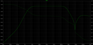
you have light peak at point A at 250kHz...
the current through R1 is hm, problematic...
Attachments
I didn't use that gain stage because the output swing is a bit limited for a high power tringlotron.cross gain stage like in the file from attachment:
For headphones, it doesn't matter: the power is ample enough.
You are not supposed to look at point A.Elvee
you have light peak at point A at 250kHz...
It is an internal test point to be used solely by the designer.
The user may just look at the overall frequency response.
should have deleted that *$£* TP
What is problematic? The notch at ~10MHz?the current through R1 is hm, problematic...
It is caused by the slow OP transistors and the various additional degenerations combined with the error correction. At this frequency, the weak residual output signal becomes completely out of phase with the correction, hence the null.
Note that it is almost completely a simulation artifact: in reality, it is unlikely you could observe something that clear-cut.
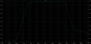
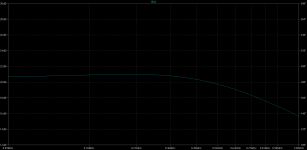
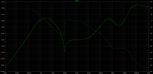
You should indicate the source of your graphs, things would be clearer.... and if AC=0 we got this...
the circuit needs modifications
but anyway I like it very much!
I think what you show is the PSRR, see below.
In that case, no modifications are needed: it is entirely intentional.
Unlike many SE-Class A amplifiers, the Tringlophone is designed to be used directly with a raw, moderate quality supply, and doesn't need a gyrator or regulator: the PSRR over the audio band is decent, and in addition a notch is located at 100Hz to increase the ripple immunity.
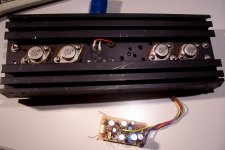
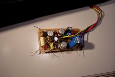
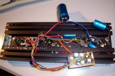
Here are some pics of my prototype:
Attachments
Sounds sweet and nice (do you really expect I'd say something else?...And how do you like the sound?
Let's wait for other, independent opinions)- Status
- This old topic is closed. If you want to reopen this topic, contact a moderator using the "Report Post" button.
- Home
- Amplifiers
- Solid State
- ♫♪--My little posh Tringlophone--♪♫