Let us have a closer look at the Tringlotron OP.
Compared to the basic topology described in the article, there are two main differences:
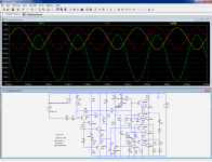
The operation is illustrated in the first pic below: the green trace is the 2Â output current, which is easily supplied using only 1.6A average quiescent current: red trace, Q6's collector current. When a current excursion is needed, the peak reaches 2.6Â.
As a side effect, this also means that Q8 has a lighter job to do: the yellow trace shows an excursion only half that of the green trace.
However, it is important to understand that Q8 is the sole output device: it is "helped" by the current modulation, but does not request nor need it: if the modulation is turned off, the operation of the circuit remains completely identical, except of course that clipping takes place if the peak output current exceeds 1.6A.
This means that the Tringlotron operation is not affected by the modulation, and the modulating path doesn't need to be clean or linear: the noble path is under the full control of the three transistors in the tringle.
The modulation simply improves the efficiency.
Even with this trick, the actual efficiency remains pretty low: in theory, it could reach 50% at full power, but in fact it is closer to 25% due to the various overheads and margins required for both voltage and current.
Each transistor needs a minimal Vce to operate properly, and there has to be some current margin to account for the real-life impedance of the speaker: unlike class B, class A requires to plan in advance the use of the current.
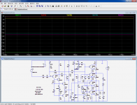
To ensure proper operation and minimize the losses, the voltages along the tringle have to be set very carefully, in order to make an optimal use of the supplies.
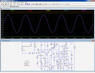
This is shown in the next two pics, first the quiescent levels for each collector and emitter, then the same with a near-maximum signal applied.
In the tringle, the "error" (non-linearity) caused by Q12/Q13 is corrected by an anti-error appearing at Q10/Q11.
No it is not a typo: it looks counter-intuitive, but that is the way the circuit works: upside down.
When Q11's base is pulled lower, its collector current decreases: the opposite of a regular follower; this creates a negative input resistance and explains the need for R12/C6.
This means that ideally, Q10/Q11 and Q12/Q13 should be matched. In fact, the behavior of the NPNs is almost completely hidden by the PNP inputs, and as a consequence only Q11 and Q13 need to be matched (for maximum linearity; it will work perfectly without matching)
Compared to the basic topology described in the article, there are two main differences:
- The polarity is reversed (PNP composites). This poses no particular difficulty of comprehension.
- The current source is not fixed, it is modulated by the signal: this creates the adaptative SE class A.
The operation is illustrated in the first pic below: the green trace is the 2Â output current, which is easily supplied using only 1.6A average quiescent current: red trace, Q6's collector current. When a current excursion is needed, the peak reaches 2.6Â.
As a side effect, this also means that Q8 has a lighter job to do: the yellow trace shows an excursion only half that of the green trace.
However, it is important to understand that Q8 is the sole output device: it is "helped" by the current modulation, but does not request nor need it: if the modulation is turned off, the operation of the circuit remains completely identical, except of course that clipping takes place if the peak output current exceeds 1.6A.
This means that the Tringlotron operation is not affected by the modulation, and the modulating path doesn't need to be clean or linear: the noble path is under the full control of the three transistors in the tringle.
The modulation simply improves the efficiency.
Even with this trick, the actual efficiency remains pretty low: in theory, it could reach 50% at full power, but in fact it is closer to 25% due to the various overheads and margins required for both voltage and current.
Each transistor needs a minimal Vce to operate properly, and there has to be some current margin to account for the real-life impedance of the speaker: unlike class B, class A requires to plan in advance the use of the current.
To ensure proper operation and minimize the losses, the voltages along the tringle have to be set very carefully, in order to make an optimal use of the supplies.
This is shown in the next two pics, first the quiescent levels for each collector and emitter, then the same with a near-maximum signal applied.
In the tringle, the "error" (non-linearity) caused by Q12/Q13 is corrected by an anti-error appearing at Q10/Q11.
No it is not a typo: it looks counter-intuitive, but that is the way the circuit works: upside down.
When Q11's base is pulled lower, its collector current decreases: the opposite of a regular follower; this creates a negative input resistance and explains the need for R12/C6.
This means that ideally, Q10/Q11 and Q12/Q13 should be matched. In fact, the behavior of the NPNs is almost completely hidden by the PNP inputs, and as a consequence only Q11 and Q13 need to be matched (for maximum linearity; it will work perfectly without matching)
Attachments
By the hell, Elvee,
why are-you using the awful 2N3055, the worse power device ever for audio ?
Experience have taught-me that quality of any amp is proportional to his speed. Why do not use the fastest devices you can find ?
Yes i know, Error correction is not so sensible to open loop bandwidth than global FB (shorter loop), but i'm sure that better BJTs will bring-you less TIM, and less high order harmonic, both with a better phase response.
Craptanium rather than unobtanium prove magic of the design, not of the parts.
Worst case devices are obviously not a requirement forced upon every builder.
But if you are exploring error correction, why not test your deviousness against
something with an obvious error to fix? 2N3055 becomes the optimal choice.
Worst case devices are obviously not a requirement forced upon every builder.
But if you are exploring error correction, why not test your deviousness against
something with an obvious error to fix? 2N3055 becomes the optimal choice.
Last edited:
Hi, kenpeter. I have tried error correction long years ago, in a very different configuration. (Symetrical output stage, differential input/output comparator). Since that time, i have a great respect to the error correction principle. So i don't need to be convinced any further about that.
My remark was not ironic against Elvee, on the contrary. If his goal was to demonstrate, you're right.
But why not trying the best as possible from the start, trying to remove in the same time those sad condensers in the signal paths, and make a high end audio amp ?
I ask myself a question too. Considering the power stage with an error correction as a near perfect power device, what happens if we build a closed loop amp with it, adding, for example, global Current Feedback ?
How does the two feedbacks can react together and dispatch their action ?
*Thanks to Bob CordellI have tried error correction long years ago
")
There are several good reasons not to, IMHO. We have one reason already in proving the design, not the parts or extraneous circuitry. Mostly, designs seen in a developed state here are just adaptations of old ones with new parts and the latest popular topology - nothing is learned except some exercise in reading datasheets, judging the symmetry of simulation traces and just talk about components.....But why not trying the best as possible from the start, trying to remove in the same time those sad condensers in the signal paths, and make a high end audio amp ?.....
Newbs will always ask if they can have PCB patterns or use craptanium parts because that's all they can buy, so it is great encouragement to beginners and experienced guys alike to get to work and do the polishing up, etch pretty PCBs and use hi-speccium parts for themselves, if they wish. That's sharing an opportunity for real DIY and learning, I think.
Last edited:
There are very few true error-correcting schemes around.Hi, kenpeter. I have tried error correction long years ago, in a very different configuration. (Symetrical output stage, differential input/output comparator). Since that time, i have a great respect to the error correction principle. So i don't need to be convinced any further about that.
Most so-called "error-correctors" are in fact some kind of NFB in disguise. This includes Cordell and Hawksford. This is not to say these schemes are worthless or ineffective, they do improve the linearity, but there is an intellectual dishonesty in calling them so: in principle, true error correction is capable of cancelling error completely, whereas feedback can only reduce it by the loop gain.
Yet the proponents of these schemes claim the total cancellation is possible, which it isn't.
In general, it boils down to a local feedback loop, or some bridge configuration, or a "comparator" as in your example: that's where the loop gain is hiding.
This means that these "EC" schemes are subject to the constraints of closed loop systems, in particular stability. No loop gain = no correction.
Obscuring the NFB aspect is dangerous, because it hides the issues associated with it, and it leads to needlessly complicated schemes, where accurate balance between passives is required for instance, when it is not actually needed if the same system is implemented in a more rational way, with NFB explicitly shown and accounted for.
That said, local loops and hierarchical nesting of NFB does have many advantages, but it is something else.
That is perfectly possible: an error-corrected stage is a very clean and well-behaved building block, and if you add plenty of loop gain to a natively ppm level OP, you can end up with a ppb level amplifier (even using lousy 2N3055s as OP)I ask myself a question too. Considering the power stage with an error correction as a near perfect power device, what happens if we build a closed loop amp with it, adding, for example, global Current Feedback ?
How does the two feedbacks can react together and dispatch their action ?
Yes, my first experiments (long time ago) where in the spirit of Cordell. And, some time later, near this one:There are very few true error-correcting schemes around.
Most so-called "error-correctors" are in fact some kind of NFB in disguise. This includes Cordell and Hawksford.
PM-AB1 error correction amplifier
And, yes, thinking to that, it is "some kind of NFB in disguise", you're damn right.
To be honest the schematic you posted is pretty complicated (means not familiar to me) and i will need some time to analyze and understand-it.
May-i suggest-you to write a little 'theory of operation' ?
The operation of the circuit can be demonstrated by simply writing down the Kirchhoff's laws, but it probably does little for the actual understanding.May-i suggest-you to write a little 'theory of operation' ?
Let us try to do it in a pedagogic and intuitive way. There is no need to mess up with the complete schematic for the moment, the principles remain the same as for the simplified circuit:
An externally hosted image should be here but it was not working when we last tested it.
Let us do it in two passes: first, the progression of the AC signal without consideration for the error signals, and then the analysis of the error voltages.
Starting from Vin, the signal is copied from Q1's B to E, is applied to Q2 through D1 and drives the top side of the load. Since Q3's B and E are at a zero potential in AC, the voltage is applied across the load and generates a current into Q3's E which is transferred to its collector and from there passes through Q1 to loop back at the top of the load: we have looped the loop encompassing Q1, the load and Q3.
Now, let us look at the error voltages generated along this path. The error voltages are caused by the BE non-linearity.
Two identical voltages are generated in Q1 and Q3 (neglecting the Hfe, the current is the same everywhere in the loop). The error voltage in Q3 is "normal", ie the product of the emitter current by the non-linear dynamic emitter resistance is subtracted from the voltage applied to the load.
The error voltage in Q1 is identical, but it is applied "upside down" to the top of the load: Q2's base is connected to the emitter of Q1.
This creates a subtraction of the error voltages as seen from the load.
There is still another possible error voltage in the loop, the BE of Q2. But since the AC current in Q2 is zero, so is its error voltage and the error cancellation between Q1 and Q3 is perfect. Neglecting higher order effects, like finite Hfe and Early effect, of course.
Compensations could be included for these effects, like in multi-transistor CCS's, but it is probably simpler to use devices like MOSFets having a negligible input current.
As a side effect, because the voltage appearing across the load is exactly Vin, independent of the output current, this implies that the output impedance is zero.
Last edited:
Brilliant.Let us try to do it in a pedagogic and intuitive way.
Well, this suppose that you are able to find 3 similar power units witch behave exactly the same, and that you are able to get the base of T1 tracking exactly the voltage changes of the emitter of T2 (perfect zener here). So the result will depend a lot of the pairing process.
This idea (new for me) suffer 3 major inconveniences.
- This is class A with extra losses.
- I don't see at first sight how it would possible to make a symmetrical circuit of it.
- Neither to remove the cap in the HP line.
In fact, when you said error correction was inappropriate for Cordell and Hawksford's schematics, i disagree. In fact, it is this one that i would see with an other name, like "Error compensation" ;-)
Bearing in mind that the design is supposed to be unique, normalizing via debate is not interesting at all. However, I'm assuming that an upgrade output device shouldn't be too difficult.
Hi Elvee. To help Esperado, which of the following "3055 replacements" would you say is an upgrade: MJE3055, MJW18020, 2SD1047, MJ15022, MJ15024, MJ*21196, MJ*21194, MJ15003?
Or, a totally weird way to ask that question, and so we're not tempted to shop for overdo, what speed does the output device need to go to be barely faster than the amp?
Last edited:
I believe that any BJt with a FT > 10Mhz would fit if you use an additional global loop with the previous stages. The faster, the better. If not, 1Mhz will feat.Bearing in mind that the design is supposed to be unique, normalizing via debate is not interesting at all. However, I'm assuming that an upgrade output device shouldn't be too difficult.
Some 3055 are fast enough, my remark was half humorous, back 30 years ago, in a cemetery of 3055, faster to burn than to reproduce a 10Khz signal. I hate them forever.
Wow!, That's fast and nice.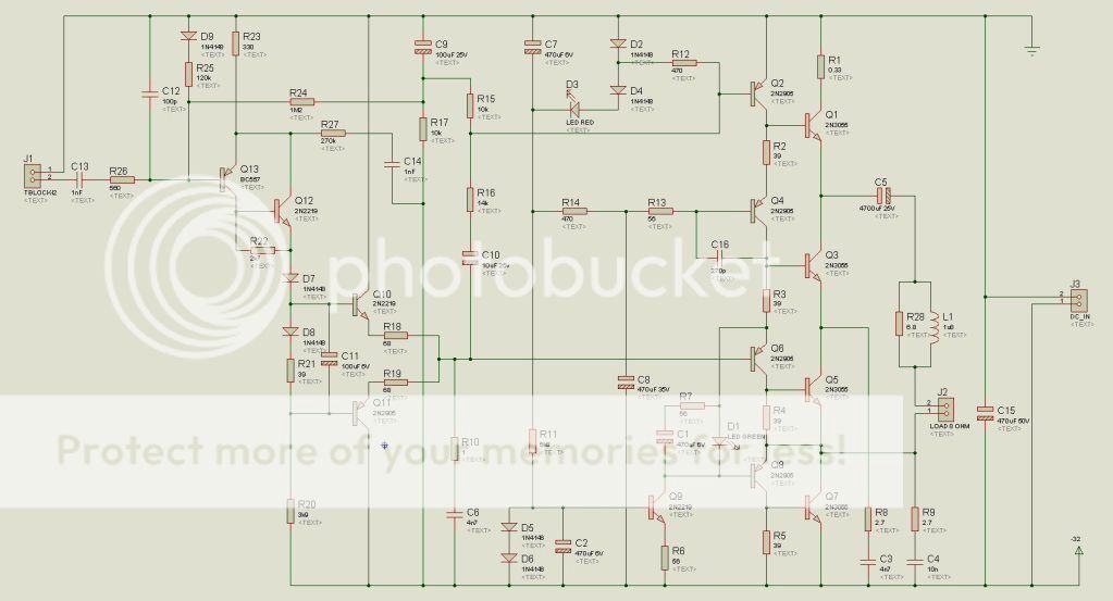

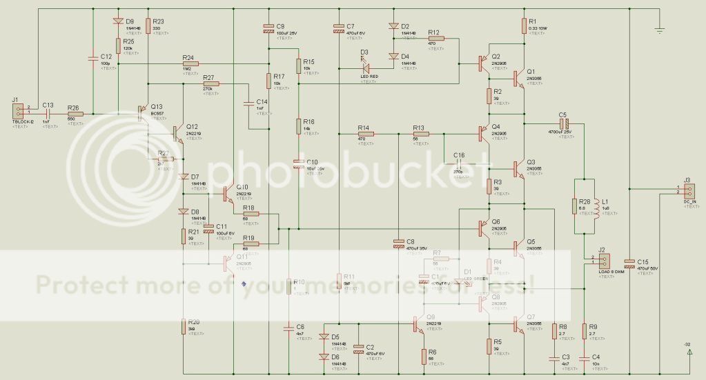
Errors? Problems with fitting a heatsink? Different connectors? Different positioning?
A few remarks:
The emitters of Q2, Q4, Q6 should go to the collector of their respective NPN
R1 must be capable of dissipating 1W at the very least; preferably 1.5 or 2W.
There has to be room enough to attach a substantial heatsink. Some components like C5, R1, R3, R4 are probably too close.
Otherwise, it should be OK
Thanks!Elvee?
I won't be building it but I don't mind laying it out and posting the gerbers.
I will stop when I find some spare time to die....Another piece of original development Elvee, you just don't stop, do you?
You do not need 3 matched power transistors: first, in a CFP, the input transistor dominates and ultimately dictates the behavior of the composite (don't push it too far though: this doesn't mean you are allowed to mix different types of transistors).Brilliant.
Well, this suppose that you are able to find 3 similar power units witch behave exactly the same, and that you are able to get the base of T1 tracking exactly the voltage changes of the emitter of T2 (perfect zener here). So the result will depend a lot of the pairing process.
Second, only Q1 and Q3 require matching. Q2 has little effect, and that is the way it should be: ideally, it should display a minimal Early effect in order not to interfere with the correction.
The perfect zener is not a problem: it can be bypassed, as in the tringlophone.
That is a (true) class A amplifier: if you want class A you must also accept the power dissipationThis idea (new for me) suffer 3 major inconveniences.
- This is class A with extra losses.
The buffer UniGaBuf uses the same fundamental correction principle, but implemented in a very different, class B-like topology.
It is possible: I have done it. I have chosen to publish this version, because the symetrical version is even more part-intensive: it requires a total of 6 OP devices, including the CCSs.- I don't see at first sight how it would possible to make a symmetrical circuit of it.
With the symetrical version, the cap can be removed. But it is not that inconvenient, and it provides free DC-protection- Neither to remove the cap in the HP line.
I will try to plug some faster devices into my prototype. Some corrections might be needed in the stabilization networksI believe that any BJt with a FT > 10Mhz would fit if you use an additional global loop with the previous stages. The faster, the better. If not, 1Mhz will feat.
All except the MJE3055 should be an upgrade, but the 2SD1047 might be difficult to tameHi Elvee. To help Esperado, which of the following "3055 replacements" would you say is an upgrade: MJE3055, MJW18020, 2SD1047, MJ15022, MJ15024, MJ*21196, MJ*21194, MJ15003?
Last edited:
I'm very curious to see it. Can-you try to define the sonic character difference, comparing to more classical global feedback based amps, if some can be characterized ?It is possible: I have done it. I have chosen to publish this version, because the symetrical version is even more part-intensive: it requires a total of 6 OP devices, including the CCSs.
Changes:-

R1 changed so that a RES60 or larger can be accommodated.
For the heatsdinking, I suggest aluminium U- or L-section, can be sectioned or 1-piece with thermally conductive insulators, trapped between Q1-Q7 and board.
The additional holes provided mean that, with a little bit of effort, a board capable of being used with any off-board heatsinking and mounting arrangement for the 2N3055s (or WHY) can be economically produced, even for submission to a manufacturing facility with a little editing of the gerbers, which can probably be accomplished in GCPrevue.
Although no output connector is shown, an RCA input and DC bullet connector footprints are provided, although there is nothing to prevent a user wiring in any kind of chassis-mount connector.
View attachment tringlophone - CADCAM.ZIP
Here's some of the newer devices: NJL3281 MJL3281 FJL4315 NJL4281 MJL4281 At least it could demonstrate that output device speed in excess of the amp speed, is either turned into HF noise or "tamed" by going even slower than before. Isn't that about how it goes?All except the MJE3055 should be an upgrade, but the 2SD1047 might be difficult to tame
So, actually, I might be shopping for MJ15003? (doesn't need an amp rework) and trying for a ~17 watt amp phase linear up to 1Mhz? Or maybe more like 15W with the MJ21194 if phase linear to 3.5Mhz doesn't incur a lot of added transistors? Somewhere in that ballpark?
That looks fit enough for trial.Changes:-
R1 changed so that a RES60 or larger can be accommodated.
For the heatsdinking, I suggest aluminium U- or L-section, can be sectioned or 1-piece with thermally conductive insulators, trapped between Q1-Q7 and board.
The additional holes provided mean that, with a little bit of effort, a board capable of being used with any off-board heatsinking and mounting arrangement for the 2N3055s (or WHY) can be economically produced, even for submission to a manufacturing facility with a little editing of the gerbers, which can probably be accomplished in GCPrevue.
Although no output connector is shown, an RCA input and DC bullet connector footprints are provided, although there is nothing to prevent a user wiring in any kind of chassis-mount connector.
View attachment 307344
I have made some tests with a variety of devices, mainly faster ones.Here's some of the newer devices: NJL3281 MJL3281 FJL4315 NJL4281 MJL4281 At least it could demonstrate that output device speed in excess of the amp speed, is either turned into HF noise or "tamed" by going even slower than before. Isn't that about how it goes?
So, actually, I might be shopping for MJ15003? (doesn't need an amp rework) and trying for a ~17 watt amp phase linear up to 1Mhz? Or maybe more like 15W with the MJ21194 if phase linear to 3.5Mhz doesn't incur a lot of added transistors? Somewhere in that ballpark?
To my astonishment, it worked immediately, without even tweaking the degenerations and stabilization networks.
I guess I may have been somewhat heavy-handed in that department, as I wanted to remain on the safe side.
The devices tested were BD317, 2N5886, BDY58 and RCA 41013 and 64116 (I think it is broadly similar to the 2N6340).
Except for the 64116, I only replaced the two main transistors involved in the tringlo action, as I had only one sample pair of each type and the auxiliary transistors play a minor role.
I also noticed that on my prototype, the 47n C14 was left in place as in V5d.
This probably helps.
When the amp is pushed into clipping, a VHF oscillation is visible with the faster types, but nothing dangerous or alarming.
This means that the new Onsemi types should work transparently.
Oh, congrats!
It looks like Class A didn't have all those switching caveats?
Does Tringlophone max out at 11 watts, or could we aim a bit higher? Maybe this affects the output device choices a bit?
P.S.
The ClipNipper was designed for a 10 watt to 8 ohm amplifier, and if using it for 11 watts, can just exchange its 1N5819 for a standard diode. That circuit (in my signature, 1st post schematic) will make Tringlophone exchange clipping for compression instead, just like a tube amp. That's borderline enough for a recording of a piano to play as loud as the real thing. To get it the rest of the way to impressive, an 11 watt amp needs some efficient woofers. Its doable.
It looks like Class A didn't have all those switching caveats?
Between MJW18020 to MJW4281 there's an HFE difference. Do you prefer relatively low, medium, or high HFE outputs. . . and what amperage figure should I look at on the HFE vs amperage charts?This means that the new Onsemi types should work transparently.
Does Tringlophone max out at 11 watts, or could we aim a bit higher? Maybe this affects the output device choices a bit?
P.S.
The ClipNipper was designed for a 10 watt to 8 ohm amplifier, and if using it for 11 watts, can just exchange its 1N5819 for a standard diode. That circuit (in my signature, 1st post schematic) will make Tringlophone exchange clipping for compression instead, just like a tube amp.
That's borderline enough for a recording of a piano to play as loud as the real thing. To get it the rest of the way to impressive, an 11 watt amp needs some efficient woofers. Its doable.- Status
- This old topic is closed. If you want to reopen this topic, contact a moderator using the "Report Post" button.
- Home
- Amplifiers
- Solid State
- ♫♪--My little posh Tringlophone--♪♫