Hi subwo !
Yes, it's very likely that this cap would toast the mosfets...
(That's why i will not try it...)
I just have the problem that i have too much deadtime now,
and can't easily reduce it, as the caps are already gone.
I can't increase currents easily, without reducing the voltage to
frontend i would cook the transistors...
The design would work with limited voltagesupply for the frontend,
but needs a lot of extracomponents for voltageregulators.
So i have to find other ways to speed up the circuit, or avoid the
effect of deadtime creating distortions ?
Mike
Mike,
The Amidon type 2 Red cores are the best for Class D type Apps – the give about 0.0015% open loop 120W 8 ohms – and very little heating – even at 768KHz.
Too much deadtime will be just as bad a too little – by increasing the deadtime you allow the internal diodes to start conducting – with there VERY slow recovery times. In a well designed fast output stage, the internal heating caused by this diode can easily be worst then the energy dissipated by cross-conduction.
Another potential issue with deadtime is that the output stage is in a “Tri-State” condition, encouraging the trapped inductance around the output stage to act like mini “fly-back” converters, releasing there “trapped” energy during this “Tri-state” condition – resulting in massive, very fast ringing - and with most common Scopes (sub 1GHz) the extent of this ringing will not be appreciated (also watch the rise time of the Scope Probe). I tend to find that the ringing caused by the realise of this "trapped" energy, resulting in ringing of say 2nS - 5nS but can easily be double the rail voltage - with most Scope / Probe combinations this just appears as "Mild" over / undershoot - leaving you wondering why you can't pass EMC, your output stage causes erratic operation of other circuits (and your temperature controlled soldering station) and why your FETS fail after time.
The lowest ringing, lowest loss output stage is one where the deadtime is just enough to reduce cross-conduction to an acceptable level and no more.
When choosing the deadtime period, a sweet-spot will be found between lowest losses due to cross-conduction – and losses due to diode recovery times – so don’t be surprised to find reduced ringing and reduced losses with a SHORTER deadtime.
The real trick is to make the Driver discharge the MOSFET’s Gate charge – slow turn-on can be lived with (although not ideal) – but fast turn-off is critical.
John
JohnW,
I was wondering if you have any experience with the use of snubbers in this application. I know they reduce efficiency but sometimes there's no way around using them (of course, once you have done what you can with the dead time).
Also, has anyone considered putting schottky diodes in parallel with the MOSFET body diode? I know it is a challenge to find large current shottky diodes for high voltages, but AFAIK the body diode is a PN diode, not a schottky. A schottky would prevent it from ever conducting a large current due to it's lower forward voltage.
Some months ago Bruno or John wrote something about it. There is the possibility, that the stray and parasitic inductances e.g. of the FET's leads and traces prevent the external diodes from taking over the current. The steep di/dt will induce a voltage across the leads, greater than the forward voltage drop difference between body diodes and the external ones.
I hope to reproduce the statements right.
Regards, Timo
I hope to reproduce the statements right.
Regards, Timo
tiki said:There is the possibility, that the stray and parasitic inductances e.g. of the FET's leads and traces prevent the external diodes from taking over the current. The steep di/dt will induce a voltage across the leads, greater than the forward voltage drop difference between body diodes and the external ones.
Timo,
It must have been a posting by Bruno’s and is 100% correct.
I’ve never had call to use snubbers – so I can’t comment – however they are just a “Fix” for a bad situation….
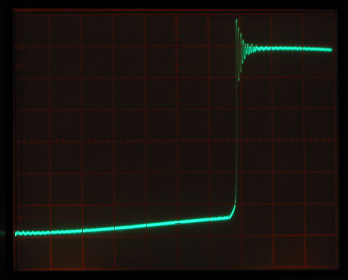
Attached is a picture of a “budget” 120W output stage – with no snubbers or tricks – its really not the greatest design (the simplest I could do at lowest cost) – however it does switch 50V in about 2nS with NO ringing – note we are looking at the Pch switch event – always the worst from the Gate charge perspective.
The Yellow (10nS / Div, 10V / Div) trace is the output swinging 50V in about 2nS notice NO ringing, the Purple trace is the Gate, also notice how the Miller charge reverse couples into the Gate and brings Vth below Ton for about 10nS (remember we are looking at a Pch device). The probes have been “time compensated”
This is not a great OPS however total cost including drivers was about US$2.20 – for a 120W 8Ohm output stage – less then 2 Cents per Watt, and distortion open-loop was still below 0.08% at full rated power.
John
Attachments

Mike,
In the circuit above I used the Vishay SUD10P06-280L & SUD15N06-90L. This circuit only used 1 Pch device, so RDSon thermal losses where higher at 120W – I used to use 2 Pch devices per HBridge side to compensate for there losses.
Over the past couple of years I have been using the Vishay Si7414 / 7415 with very good results – the Pch having much lower RDSon – requiring only one Pch device per HBridge Half.
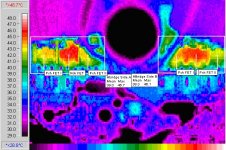
Below is a thermal image of a 2x SUD10P06-280L & SUD15N06-90 (per HBridge side) output stage, it’s been operating at 110W into 8 Ohms for 30 Minutes continues – the only heat-sinking being the 2 ounce copper PCB. Clean / fast switching, with no ringing is the secret to this performance.
John
In the circuit above I used the Vishay SUD10P06-280L & SUD15N06-90L. This circuit only used 1 Pch device, so RDSon thermal losses where higher at 120W – I used to use 2 Pch devices per HBridge side to compensate for there losses.
Over the past couple of years I have been using the Vishay Si7414 / 7415 with very good results – the Pch having much lower RDSon – requiring only one Pch device per HBridge Half.
Below is a thermal image of a 2x SUD10P06-280L & SUD15N06-90 (per HBridge side) output stage, it’s been operating at 110W into 8 Ohms for 30 Minutes continues – the only heat-sinking being the 2 ounce copper PCB. Clean / fast switching, with no ringing is the secret to this performance.
John
Attachments
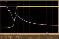
Mikeb, is that without load? Yes, I think that's too much ringing.
It can be caused by excessive inductance in the switching node, or poor decoupling of the supply lines (the caps should be very close to the mosfets).
I also wonder why do you have a not flat negative phase.
Best regards,
It can be caused by excessive inductance in the switching node, or poor decoupling of the supply lines (the caps should be very close to the mosfets).
I also wonder why do you have a not flat negative phase.
Best regards,
Hi Mike,
You don’t give a V/Div for you scope image – so it’s impossible to comment – also what type of scope/probe you are using – if you’re using a 100MHz type scope then it most likely will be much worst – but I would be unhappy with the ringing…
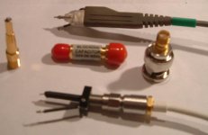
The trick with probing fast rise-time signals is to use a Scope Probe with a very short Ground connection next to the Tip,
Below is a poorly focused picture (my camera does not have a decent “macro” function),
Top to bottom: -
Tek P6245 1.5GHz active prove – ok to about 15V, notice how both the Ground lead (the head is laying in it) and probe tip can be soldered directly to PCB – for fine SMD work
TEK P6150 resistive probe tip (Gold object – on the left corner of the picture) – limited to 12.5V RMS, very fragile “Tip” and no easy way to attach to PCB – but good to 9GHz and above
DC block & BNC to SMA for scale
HP54006A Resistive Probe (with X10dB Head (450 Ohm resistor)) I use this with 60V swing output stages – easy to solder to PCB – good for 6GHz+ A Great probe for OPS work.
I guess that with a decent piece of COAX and a 450 Ohm resistor (the HP54006 x10 head uses a Caddock MD1247 450R 1%) you could construct your own 50Ohm HF probe.
Cheers,
John
You don’t give a V/Div for you scope image – so it’s impossible to comment – also what type of scope/probe you are using – if you’re using a 100MHz type scope then it most likely will be much worst – but I would be unhappy with the ringing…
The trick with probing fast rise-time signals is to use a Scope Probe with a very short Ground connection next to the Tip,
Below is a poorly focused picture (my camera does not have a decent “macro” function),
Top to bottom: -
Tek P6245 1.5GHz active prove – ok to about 15V, notice how both the Ground lead (the head is laying in it) and probe tip can be soldered directly to PCB – for fine SMD work
TEK P6150 resistive probe tip (Gold object – on the left corner of the picture) – limited to 12.5V RMS, very fragile “Tip” and no easy way to attach to PCB – but good to 9GHz and above
DC block & BNC to SMA for scale
HP54006A Resistive Probe (with X10dB Head (450 Ohm resistor)) I use this with 60V swing output stages – easy to solder to PCB – good for 6GHz+ A Great probe for OPS work.
I guess that with a decent piece of COAX and a 450 Ohm resistor (the HP54006 x10 head uses a Caddock MD1247 450R 1%) you could construct your own 50Ohm HF probe.
Cheers,
John
Attachments
Hi Mike,
“Few cm away from the MOSFET’s” Wow – that might as well be KM away….
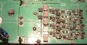
Here’s picture of one of my typical output stage designs - 120W full bridge – note I’ve blown one pair of output devices and these have been removed (the lower pair in the picture - now just exposed solder pads), along with a decoupling cap.
But notice how I have 1uF 1210 HF grade ceramic decoupling CAPS as close as physically possible to the MOSFETS – these caps decouple the output devices on each HBridge half side AND across the bridge (load current flows across the bridge).
The MOSFET devices are the VISHAY – SILICONIXS Si7414 /15, and notice the Limited PCB heatsinking required for 120W 8 Ohms. (The SMD SO8 device sitting near the "Heatsink PCB area" is there for "Scale" only)
Cheers,
John
“Few cm away from the MOSFET’s” Wow – that might as well be KM away….
Here’s picture of one of my typical output stage designs - 120W full bridge – note I’ve blown one pair of output devices and these have been removed (the lower pair in the picture - now just exposed solder pads), along with a decoupling cap.
But notice how I have 1uF 1210 HF grade ceramic decoupling CAPS as close as physically possible to the MOSFETS – these caps decouple the output devices on each HBridge half side AND across the bridge (load current flows across the bridge).
The MOSFET devices are the VISHAY – SILICONIXS Si7414 /15, and notice the Limited PCB heatsinking required for 120W 8 Ohms. (The SMD SO8 device sitting near the "Heatsink PCB area" is there for "Scale" only)
Cheers,
John
Attachments
MikeB,
Any progress? Or are your stuck? Maybe JohnW can give some pointers he seems to be very knowledgable about the subject.
Best regards,
Sander Sassen
http://www.hardwareanalysis.com
Any progress? Or are your stuck? Maybe JohnW can give some pointers he seems to be very knowledgable about the subject.
Best regards,
Sander Sassen
http://www.hardwareanalysis.com
MikeB, I have used with success a standard 100MHz oscilloscope probe. But it is VERY important that you use the HF accesory (a special tip that has a very short ground pin to avoid a pickup loop).
With this, measuring just at the mosfets leads, you should see all you need to see.
Why do you have so small bypassing of the supply lines, MikeB? You should have a good ceramic cap as well as some tens of uF good electrolytics as near to the mosfets as possible.
Best regards,
Pierre
With this, measuring just at the mosfets leads, you should see all you need to see.
Why do you have so small bypassing of the supply lines, MikeB? You should have a good ceramic cap as well as some tens of uF good electrolytics as near to the mosfets as possible.
Best regards,
Pierre
Hi !
Hmm, i thought they should be enough to store the emf from choke,
but they are obviously too small, as the voltage rises several volts...
I use wima-mks2 now, i don't know if ceramics are better ?
I've read that these wima are better than ceramics, but i might
have been fooled...
At least these caps are the only devices keeping cold !
I just gave this project a break, i will continue later and replace
the driverstage with something more sophisticated...
At the moment i am busy with some promising ClassAB.
BTW, i replaced the outputchoke with a amidonring-version, but
did not change much. The fuses still run hot... Maybe skineffect ?
This should be reducable by using larger supplycaps.
The scope is a tektronix 475, capable of 200mhz, the probe has
a ~10cm ground-wire.
Mike
my BJT gate driver used 1K pullup resistor and a single 2SC8050 (fT=100MHz) for emitter follower. The gate waveform is crappy.
How many stages of emitter follower should I cascade? (Yours: 2 stages)
Too less=low gain, but too many=too big propgation delay?
How many stages of emitter follower should I cascade? (Yours: 2 stages)
Too less=low gain, but too many=too big propgation delay?
MikeB said:Oh, bjts beeing able to supply more than 10amperes have "slightly"
higher capacitances... And reach at least ft of 50mhz. The transients
for these squarewaves are equivalent to frequencies above 25mhz,
giving a currentgain of 2 (hfe)... This makes these devices useless !
Also, a mosfet costs around 60cents, a powerbjt 5$...
And transistors don't like it too much to be reversebiased.
There are many reasons why mosfets are far superior for ClassD.
Even these "small" mosfets can work with peakcurrents up to 100A !
Modern mosfets have inputcapacity below 500pf and outputcapacity
of 40pf ! A mjl3281 has outputcapacity of 600pf !
Mike
- Status
- This old topic is closed. If you want to reopen this topic, contact a moderator using the "Report Post" button.
- Home
- Amplifiers
- Class D
- My fully discrete ClassD