Maybe it's time to ask Santa for a new Fiancé.
Nah, She's the best.
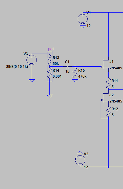
Let's fix one thing at a time, please. Sims are not needed, it's a very simple circuit.
Just wire your buffer as shown in the attached schematic, nothing more connected and report.
r15 can be 330k to 1meg and c1 value isn't critical for now. Don't mind the 2n5485, that's all I had as model installed on this computer.
Thank you, I will change the board accordingly.
the input in post38 is correct.
R15 sets the input impedance.
C1 is the DC blocker.
Compare to post30.
R14 sets the input impedance. do you really want 1k8 as your input impedance?
C2 is in the wrong position.
What is R2 =10k supposed to do?
This input is completely wrong.
Move C2 to next to R2
Change R2 to 2k or 100r or anywhere in that range.
C6 is the RF filter. For simulation of the circuit set it to 1fF
For filtering simulation set it to around 200kHz, i.e. RC = ~0.5us (500ns), 10k+6k5 & 100pF = 1650ns
I'll have to read this one a few times.
Thanks to you as well for your help
")
I suggest you disable the dc servo until after you have analysed the circuit and understand what each section and it's components do.
I suggest you remove one Rtrim = 68 and replace with a fixed 68r. That sets the basic CCS is around 9 to 10mA.
OOPS. this bit is wrong:
Multiply by Vcc = 15V
The voltage across the inputs is NOT 15V. It is ~15.6V
and you get ~150mW dissipation. That should be confirmed by the sim.
In my book that is HOT.
BC5xx have typically 500mW max dissipation.
I usually set max peak instantaneous dissipation at less than half that figure i.e. peak instantaneous dissipation <=250mW
I also set the continuous dissipation at less than half that peak, i.e. Pq < 50% of peak < 125mW
@ 15V that would be ~8mA That would require Rtrim = 81r (any value from 68r to 100r will work.
But you can choose to run your input stage hotter if you like.
The hotter you run that input stage, the more the parameters will change as the temperatures change. The DC servo will help hide some of that change.
But the BJT Buffer requires very stable Vbe values for it's good performance.
Go to the junction of Q5 collector and Q3 base.
Down the left side you have Vdrop = Vr5 + Vbeq3 and down the right hand side you have Vbeq3 + Vr7.
If both tie in to nodes at 0.0mVdc, then you have Vr5+Vbeq3 = Vbeq3+Vr7.
If you make the first stage assumption (which is not true in practice) that the two Vbe are the same, then we have Vr5=Vr7
This requires that Ir7 passes more current than Ir5. Using your 33r and 2r15 resistances you have Ir7 = 15.35*Ir5
i.e. R7 passes ~ 15times more current than R5. Your sim ratio is ~13times indicating that the Vbe are not equal. It's this current ratio that WILL CHANGE when temperatures change.
The Rtrim thus sets the output pair bias current.
BUT !!!!!! this bias current and any AC change in output voltage is VERY dependant on the two Vbe voltages. if one voltage changes then that current ratio ALSO changes.
This is where I consider that VERY stable temperatures are necessary for good performance.
I would run the input much cooler and thermally couple Q1 to Q2. And consider adding some form of heatsink. A 20mm square of 1mm thick aluminium glued between Q1&2 would be a good heatsink.
Q3 and Q4 NEED a big heatsink, to minimise temperature changes, particularly dynamic temperature changes when a high current pulse passes to the load.
Remember that Vbeq3 and Vbeq1 subtract from each other to determine the current ratio and it's the resultant that determines the current to the load.
I would run Q6 and Q7 at ~10% to 15% of the CCS current. You have ~13.7% = perfect.
Q5 & 8 need a clip on heatsink, or go to a 1W Eline type (ZTX651/751).
Last edited:
I suggest you disable the dc servo until after you have analysed the circuit and understand what each section and it's components do.
I suggest you remove one Rtrim = 68 and replace with a fixed 68r. That sets the basic CCS is around 9 to 10mA.
Multiply by Vcc = 15V and you get ~150mW dissipation. That should be confirmed by the sim.
In my book that is HOT.
BC5xx have typically 500mW max dissipation.
I usually set max peak instantaneous dissipation at less than half that figure i.e. peak instantaneous dissipation <=250mW
I also set the continuous dissipation at les than half that peak, i.e. Pq < 50% of peak < 125mW
@ 15V that would be ~8mA That would require Rtrim = 81r
But you can choose to run your input stage hotter if you like.
I've built the DC-servo in such a way that all components are on a small PCB that connects to a DIP8 socket just for that reason.
I do have 68R 0805 there atm. It was suggested that I change them to trimpots, hence I changed the schematic in preparation for that.
But you maybe ment to use a trimpot on one on of the CCS's?
Pherhaps a stupid question, but will the BCxxx still run in class A with 81R instead of 68R in the CCS?
I have not powered this design with +/-15Vdc yet, but used a temporary +/-12Vdc supply.
With that I thought the BCxxx got hot.
I'll do this when I get home.
In the car(not driving) on my way to get my neck nuked.
OK, hope it all goes well
OK, hope it all goes well
Thanks!
I've gotten home now, it went well.
Though when they tell you to be perfectly still, it's suddenly the hardest thing in the world lol.
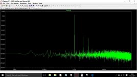
Jfet are perfectly matched in spice.
This is the big problem in simulation. I've often though it would be useful to have a set of slightly different versions of the same device to make for more accurate sims.
This is about as low a distortion figure as I can get this design for 100mw into 33 ohms.
Attachments
If that is true then he has ~-80dB 2nd and ~-100dB 3rd and no higher harmonics.This is the big problem in simulation. I've often though it would be useful to have a set of slightly different versions of the same device to make for more accurate sims.
This is about as low a distortion figure as I can get this design for 100mw into 33 ohms.
That should sound "clean".
That part does not matter, They are both jFETs that have an enormous input impedance. It's the passive components around that input that determine what signal gets into the jFETs.With this, but 2SK170's..............
It seems that this type of circuit is fairly tolerant of jFET type.
Some use high gm type, some use low noise type, some use low gm type, some use RF type.
They all seem to work.
It's when you come to inputting ultra low signal levels and want to preserve S/N ratio that type becomes critical.
I wonder if the "hot" means you have wired it up incorrectly, or that it is oscillating? Do you have a scope?...........................
Pherhaps a stupid question, but will the BCxxx still run in class A with 81R instead of 68R in the CCS?.................
And yes you ONLY need to make one 68r adjustable. When the input offset from the jFET Buffer is actually set to ZERO then the output of the BJT Buffer should read ZERO. The ONE VR allows you to set the output offset.
The DC servo makes this automated after you have it operating with zero offsets during the set up phase.
BUT !!! and this is very important. The DC servo is NOT there to balance out offset sent from a faulty Source.
You need a DC detect and mute the input if the DC servo runs out of range.
A window comparator on the servo's output that detects opamp output getting close to it's supply rail should activate a warning light/Klaxon and then a mute on the input if you don't get to the OFF switch quickly enough.
Otherwise you damage your headphones. And maybe your ears.
The CCS set the quiescent current through the two input transistors.
They can't go any higher current. They can go lower current.
The "AC output" is actually a variation in current, it's (Iq +0 -90% of Iq).
The intent is that it nevers gets to less than 10% of it's Iq. That's when it is starting to leave ClassA. You can look at the minimum current at instant moments in time for short duration pulses into the input. You should discover that it takes very high pulse voltages that happen very quickly to make the transistors turn off (or nearly off). When you look at the combination of voltage and rise time you should find they are impossible audio signals.
I don't know LTspice, but I think you should be able to analyse that, to SEE what happens and what weird combination of speed and level are needed to nearly cut off the Q1, or Q2.
Ask Mooly very nicely to add this analysis to his LTspice Thread (if it's not already in there).
Last edited:
Why do you have rtrim_50r set at 10r ? It should be 5.1 as r1. Jfet are perfectly matched in spice.
It's normal that you don't have much ac, the simulated pot is set to min volume.
I've been cautious not to feed the jfet's too much current, that is why I've set the trimpot so low.
In all honesty I've been afraid to fry the matched quad.
The problem is that you can only have 0v dc if the resistors are the same. If you're worried about killing your fets, then use 10R in both positions. If the jfet are matched, you really don't need a trimmer in that position btw, it should be good enough with two resistors.
Last edited:
The problem is that you can only have 0v dc if the resistors are the same. If you're worried about killing your fets, then use 10R in both positions. If the jfet are matched, you really don't need a trimmer in that position btw, it should be good enough with two resistors.
The circuit was originally intended as a discrete opamp.
The trimpot used to trim down DC offset.
How closely matched they are? Don't know, they are all marked 3.7mA.
I read and take in every piece of advice I get, trust me.Well, you don't have a discrete opamp. You have a weak buffer with a high impedance input feeding a stronger buffer with a lower impedance input.
Both buffers can have low offset: the jfet buffer by matching the fets/resistors and the diamond buffer by adjusting the ccs.
I'll need to sit down tomorrow and re-read it all and get an understanding for it all.
It sounds like you are having fun anyway
I am
And, I learn so much.
A few months ago I had never dreamed of building with transistors, it seemed way above my skill. I hadn't used LTSpice some months ago either.
Thanks to the very good guide I'm slowly getting the hang of LTSpice and having alot of fun using it.
New day, coffee almost in effect, new energy
A couple of questions.
1. It was written in an earlier post that the jfet is a weak buffer or similar.
How do I set higher gain for that?
2. I am going to build an opamp input stage as well. I have a few to chose from(I'm not very familiar with what opamp is good for what):
AD797(soic8, don't remember letters after AD797), OPA627AU(bought several years ago on ebay, real or not I don't know), AD8066ARZ, OPA2111KP, OPA604AP, LT1360, LT1112, LT1077, OP282GSZ, NE5532 (philips and siemens marked), OPA2134, OPA2604. I have atleast two of the single opamps.
3. Related to above question. I know it depends on which opamp/opamps I use, but where do I find a good schematic? I know from what I've read that for instance AD797 needs some additional parts/different schematic to be stable.
4. Powered on the "original" BCL clone yesterday, tired as I was the board got inverted supply for about 1s nothing blew (caps etc look ok, can't tell about BJT's). Corrected the error. I get <5mV on one channel, >180mV on the other. I have a lot of spares of the BJT's used(BC550/560, BD139/140) should I swap for new ones all around to make sure? Could actually swap the 100pF caps for wimas while I'm working on the board.
The dual rail LT1083CP reg board is set to +/-15Vdc +/-0.02Vdc. I thought that would be close enough.
- Status
- This old topic is closed. If you want to reopen this topic, contact a moderator using the "Report Post" button.
- Home
- Amplifiers
- Headphone Systems
- "My" first design headamp, DC-servo question