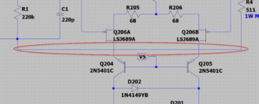
On a new simulation subject, I wanted to do simulations after inserting the HBR resistor R14. So I start by modifying my drawing to connect the joint between the input ground and the R4 ground, as a first step, and since the connection is replaced, I get a totally different plot! What am I missing there?!!
Original schematic:

Ground replaced with a line (there are no connection to the transistor emitters):

Original schematic:
Ground replaced with a line (there are no connection to the transistor emitters):
I don't see the Phase crossing the Gain more than once, but I admit I am a bit scare of the 1 kHz peak!
What do you think?
I'm sure Bonsai will have more valuable insight on this, but to me your 1st plot looks more or less 'normal,
and the PM value (39 degrees) is too low. PM should be at 45 or more.
GM on the other hand is unusally high (35).
From my experience, amps with simulated PM below 45 degrees, are very likely to oscillate, perhaps not all the time, but in certain conditions.
Grounding issues, loops, and long/convoluted PCB traces can make it even more likely.
I would aim for closer to 60 dgrees in this case (this topology definitely can achieve this).
minek123, the first plot isn't my design! It is the result from the ZIP file tutorial I download at your post #157 !your 1st plot looks more or less 'normal,
and the PM value (39 degrees) is too low. PM should be at 45 or more.
GM on the other hand is unusally high (35).
My design plots are the second and third. The second is the one to analyse as the third was just to record the peak.
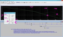
Here is another screenshot zoom. The cursor 1 is at 0dB and the cursor 2 is at the Phase crossing point. If I understand well, 180° -132° = 48° of phase margin.
Stupid me! lolYou have no connection to Ground
The fully balanced front-end and VAS stages offer very high loop gains and therefore the opportunity for extremely low distortion. However, one of the problems is that this configuration is not DC stable. A lot was written about this and discussed by Edmond Stewart when he did the PGP with Syn08 many years ago. I have used a fully balanced front end in a VFA (see the e-Amp on my website) and avoided the problem by using resistor loading and not a current mirror load on the front-end diff pairs. What you can do in the short term if it turns out this is your problem, is just unbalance the front end by loading one side of the front-end mirrors with a resistor - 5-10% imbalance should be ok. I'll try to find the Edmond Stewart information and post it up. Randy Slone's book did not discuss this issue BTW.

This design is not from Randy Slone book, but from Bob Cordell one; Figure 14.17.Randy Slone's book did not discuss this issue BTW.
To test further, I followed the tutorial titled "Inferring Loop Gain" of page 566 of my book "Designing Audio Power Amplifiers" from Bob Cordell. I made comparison of it's tutorial and my schematic in parallel.
In it's example, he said "The gain crossover is at 400 kHz, where the OLG equals 26 dB, the normal CLG for the amplifier. Phase at this frequency is lagging by 101°, suggesting a phase margin of 79°".
So if I understand is math as 180° - 101° = 79°
In my design, I had to modify the AC analysis frequency from 1Meg to 10Meg to see the Phase crossing the Gain. But I always understood that I should check for the difference of the phase between the Gain curve at 0 dB and the point where the Phase cross the Gain curve. So in the capture below, it would be (-279°)- (-240°) = -35°
Am I right?
Here is another screenshot zoom. The cursor 1 is at 0dB and the cursor 2 is at the Phase crossing point.
Not sure what Phase/Gain crossing point has anything to do with it.
Primarily, you are interested in two points:
When gain plot (thicker line) crosses 0dB horizontal line, and when Phase plot (thinner line) crosses 180 degrees horizontal line.
See attached image.
Not when one plot crosses another.
Attachments
Sevy, the frequency at which the loop gain crosses the 0 dB gain line is called the ’unity loop gain frequency’ or ULGF. with your current compensation, it is at 5 MHz which is too high, even for a mosfet OPS. You want to set it to about 2 MHz for a practical amp. This is basically a good amp that needs a bit of tweaking wrt compensation. You could use TMC (Cordell discusses this) to good effect.
I will need to look more closely at the circuit, but I don’t see how the VAS standing current is defined - I may have missed it though.
I will need to look more closely at the circuit, but I don’t see how the VAS standing current is defined - I may have missed it though.
Good. So following your analysis, my Gain would be at 0dB around 762 kHz and my Phase would be at 180° at 4.36MHz. Am I understand it right to say that my Phase Margin is then 59°?When gain plot (thicker line) crosses 0dB horizontal line, and when Phase plot (thinner line) crosses 180 degrees horizontal line.
Anyone?I'm interested to know if it's better to use a small ceramic cap between the input signal ground and the earth point, or to put a small ceramic cap between the input signal and the input ground? I've seen quite a few amp designs that do the latter
Am I understand it right to say that my Phase Margin is then 59°?
Yes.
But see Bonsai's post few minutes ago.
Usually you put a ceramic cap of 10-50 nF from the input connector signal grounds ( which you should mount next to each other and bond the grounds to each other) to the chassis metal work. This is done for RFI purposes by making the interconnect cable and the metal amplifier chassis a single enclosure at RF frequencies. The cap must be placed right at the input where the connector is.
Last edited:
That looks simply like a low pass filter that’s relying on the source resistance (typically 50-100 Ohms) to form the R part of the RC network. It will offer some series mode RFI protection, but no common mode RFI protection which is normally a bigger problem.
Ok. So I started the simulation again, in these steps. Let me know if I got it right this time.with your current compensation, it is at 5 MHz which is too high, even for a mosfet OPS. You want to set it to about 2 MHz for a practical amp
First I plotted the ’unity loop gain frequency’ or ULGF with my original C301/C401 capacitors values; 10 pF. That reproduced the to much high 5MHz frequency that Bonsai pointed out:
Then I changed the C301/C401 capacitors values for 82pF. I reached 0dB at 2.20MHz:
Then I lowered it to the next available value, 68 pF, and I kept it. That reach 0dB at 1.96MHz:
From there, I grounded the Input and added the 1 V AC source between the Feedback resistor R6 and the MOSFETs output, as suggested in the ZIP tutorial (post #157). I kept the Vout traces and added the olg() function traces. I moved the cursor "1" to reach 0dB and cursor "2" to reach -180° on the ogl() traces. I read back the Ratio Phase : -76.70°.
Is this my Phase Margin? 76°?
@Sevy The odd shape to the Loop Gain Plot is due to the DC servo. To check, delete the op-amps. Delete the one on the right and you get a normal looking plot with 35dB mid-band LG. Delete both and you get a normal looking plot with 45dB mid-band LG. I don't know if this is real or an artifact, as the LG probe feeds multiple feedback loops here. It's telling some truth, but not sure it's the one you're looking for.
THANKS!!!@Sevy The odd shape to the Loop Gain Plot is due to the DC servo. To check, delete the op-amps. Delete the one on the right and you get a normal looking plot with 35dB mid-band LG. Delete both and you get a normal looking plot with 45dB mid-band LG. I don't know if this is real or an artifact, as the LG probe feeds multiple feedback loops here. It's telling some truth, but not sure it's the one you're looking for.
It look much better ;-)
- Home
- Amplifiers
- Solid State
- My DIY Amplifier has a small sizzling sound