Hi Kanwar
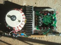
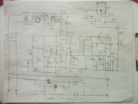
Well this is the application of the latest prototype. Transformer is a bit oversized , but it is the only one available at the time. It could power 4 more of these circuits.
 I can easily crank out ~150Wrms @ 6R despite only 4) TO-220 transistors. However, the output transistors are directly mounted onto blocks of white brass, which are energized by the rails. Each brass block is insulated with 4) TO-220 mica insulators and grease to the 1/4" thick aluminum angle piece. This reduces the effective thermal resistance of the insulators by increasing the surface area, and the brass acts as a 'thermal capacitor' due to its density. My attempt at keeping the die temperature spikes lower. The thermal compensation is done by contact of the drain pin to a small SOT-23 transistor for each OPT.
There are a few experimental sections that will not be in the final design (yet to be materialized) For example the bias control circuit. The final (hopefully) design will have fixed bias. For this one the blue pot controls bias of both output stages simultaneously using that LM358 duel op amp in the mico-8 package just behind the blue pot to servo the linear opto-couplers that are the two DIP-8 packages that interface with the error amp bias of the two seperate HEC based output stages. It works great but is not particularly necessary. In the one photo with the yellow boxes, they outlines the voltage amplifying transistors for the bridge, SOT-563 duel mosfets. I think I may be able to use J-fets in the final design, less noise. I will have to use larger SOT-23 parts though because J-fets don't seem to come in any smaller package.
The input signals are all single end. Each waveform photo with only one waveform is showing the difference of the two outputs as what the load sees.
Well this is the application of the latest prototype. Transformer is a bit oversized
, but it is the only one available at the time. It could power 4 more of these circuits. I can easily crank out ~150Wrms @ 6R despite only 4) TO-220 transistors. However, the output transistors are directly mounted onto blocks of white brass, which are energized by the rails. Each brass block is insulated with 4) TO-220 mica insulators and grease to the 1/4" thick aluminum angle piece. This reduces the effective thermal resistance of the insulators by increasing the surface area, and the brass acts as a 'thermal capacitor' due to its density. My attempt at keeping the die temperature spikes lower. The thermal compensation is done by contact of the drain pin to a small SOT-23 transistor for each OPT.There are a few experimental sections that will not be in the final design (yet to be materialized
) For example the bias control circuit. The final (hopefully) design will have fixed bias. For this one the blue pot controls bias of both output stages simultaneously using that LM358 duel op amp in the mico-8 package just behind the blue pot to servo the linear opto-couplers that are the two DIP-8 packages that interface with the error amp bias of the two seperate HEC based output stages. It works great but is not particularly necessary. In the one photo with the yellow boxes, they outlines the voltage amplifying transistors for the bridge, SOT-563 duel mosfets. I think I may be able to use J-fets in the final design, less noise. I will have to use larger SOT-23 parts though because J-fets don't seem to come in any smaller package. The input signals are all single end. Each waveform photo with only one waveform is showing the difference of the two outputs as what the load sees.
Attachments
Hmmm, odd. I was able to re-open it just fine. It is a zipx file (compressed jpeg) that is zipped again with regular .zip extention so forum would accept format.
Better to compress the images with Rar or normal Zip format, easy for us.
Hi
I don't have any of the schematics in pdf and they are all old school pencil & paper drawings. I need to get them on the PC sometime soon. Hopefully will be able to start the final PCB soon.
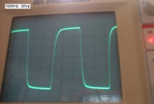
Unlike most amps I've seen on the forum this one uses planer stripe diffusion Mosfets as the output stages. Fairchild’s Q-fet line of power Mosfets to be particular, FQP50N06 & FQP47P06. Note Q-fets are not Trenchfets, the Trench types are not suitable for linear operation due to 'second breakdown like' effects. The planer stripe types have a different die structure than the cellular types such as IR’s Hexfet. Like all vertical fets, these devices were developed for use as switches and appear to be even more non-linear than the cellular types and seem to have a larger Id vs Vds dependency. However the SOA is better. They seem to be able to handle more power, and their cheap. But Hi-Fi from these transistors? Well, overall linearity isn’t a problem as indicated by the 100KHz tri. High SR, high BW, high DF, and a low noise floor. I have yet to hear an amp that will best this one, as far as sound quality goes, but I would like to try it with a range of different speakers though.
Most DIY amps are just new implementations of the same ol’ same ol’ that’s been the same ol’ for over 30 years. Why not try something a bit different? I thought. A simple novel idea….why not build a pre-amplifier circuit, that could be a complete project in itself. Then build a power amp that is a complete circuit. Optimize both of these circuits with plenty of cascodes and other linearization techniques, then direct couple the pre-amp to the power amp, slap a DC servo global loop around the whole thing and place them on the same PCB. Not only would you eliminate at least one signal coupling cap, the ‘interconnection’ wires would be very short. Sharing the same power supply is sure to simplify the circuit and eliminate GND loops with a properly designed PCB. Of course you would need voltage regulation in there for the input and VAS amplifiers, and while you’re at it, might as well throw the whole power supply in as well, eh? But then your circuit might begin to look like a PC motherboard. So what? You just build one circuit at a time, at least for prototyping. People are afraid of using transistors…….”There’s too many damn transistors in that circuit.” They always say. To that I say ‘whatever’….
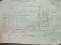
Now that I have had some time to evaluate this amp circuit and put it completely together, I suppose I can share some technical info about it. Few seem to have interest in balanced amps for some reason. Balanced amp is the way to go, IMO. I have not put effort into the looks, obviously, but I guarantee the circuitry is not like yours. Being a ‘modular’ amp with built in direct coupled pre-amp, and only 1 uf polypropylene input cap, overall Av = ~40dB. Vout is 45Vp so 0.45Vp single end input will drive the amp to full output, meaning you can use a laptop or an I-pod Nano output jack as the signal source. Gain characteristics is Av +~2dB at 20Hz, rolls off steeply at 12Hz, and rolls off back to Av at about 28Hz, sort of opposite from what you would expect from such a small input cap. Av is then flat up to ~ 480KHz. Despite having many stages in the signal path this prototype is quite fast as indicated by the 100 KHz sq wave. The outputs of the two DC servos create two separate virtual GND references related to the corresponding phase output. The gain boost at the low frequency end of the spectrum is created by playing with the LP filter value, allowing a small amount of positive feedback to the DC servos. This adds signal to the input by means of the two virtual GND references created as the output of the two servo amplifiers. This is the only global loop in the AC signal path, which spans 10 total stages (not counting cascodes) but the low pass filter is set to very slow frequency and is not affected by the overall phase margin of the # of stages. Everything above that very low audio frequency is not within a global loop, but rather each separate circuit has its own loop(s). SE to BAL conversion is accomplished by using common mode EC to correct the misbalance in the bridge caused by being driven by only one side. The jumper selects between XLR input or SE.
I don't have any of the schematics in pdf and they are all old school pencil & paper drawings.
I need to get them on the PC sometime soon. Hopefully will be able to start the final PCB soon. Unlike most amps I've seen on the forum this one uses planer stripe diffusion Mosfets as the output stages. Fairchild’s Q-fet line of power Mosfets to be particular, FQP50N06 & FQP47P06. Note Q-fets are not Trenchfets, the Trench types are not suitable for linear operation due to 'second breakdown like' effects. The planer stripe types have a different die structure than the cellular types such as IR’s Hexfet. Like all vertical fets, these devices were developed for use as switches and appear to be even more non-linear than the cellular types and seem to have a larger Id vs Vds dependency. However the SOA is better. They seem to be able to handle more power, and their cheap
. But Hi-Fi from these transistors? Well, overall linearity isn’t a problem as indicated by the 100KHz tri. High SR, high BW, high DF, and a low noise floor. I have yet to hear an amp that will best this one, as far as sound quality goes, but I would like to try it with a range of different speakers though. Most DIY amps are just new implementations of the same ol’ same ol’ that’s been the same ol’ for over 30 years. Why not try something a bit different? I thought. A simple novel idea….why not build a pre-amplifier circuit, that could be a complete project in itself. Then build a power amp that is a complete circuit. Optimize both of these circuits with plenty of cascodes and other linearization techniques, then direct couple the pre-amp to the power amp, slap a DC servo global loop around the whole thing and place them on the same PCB. Not only would you eliminate at least one signal coupling cap, the ‘interconnection’ wires would be very short. Sharing the same power supply is sure to simplify the circuit and eliminate GND loops with a properly designed PCB. Of course you would need voltage regulation in there for the input and VAS amplifiers, and while you’re at it, might as well throw the whole power supply in as well, eh? But then your circuit might begin to look like a PC motherboard.
So what? You just build one circuit at a time, at least for prototyping. People are afraid of using transistors…….”There’s too many damn transistors in that circuit.” They always say. To that I say ‘whatever’…. Now that I have had some time to evaluate this amp circuit and put it completely together, I suppose I can share some technical info about it. Few seem to have interest in balanced amps for some reason.
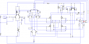
Balanced amp is the way to go, IMO. I have not put effort into the looks, obviously, but I guarantee the circuitry is not like yours. Being a ‘modular’ amp with built in direct coupled pre-amp, and only 1 uf polypropylene input cap, overall Av = ~40dB. Vout is 45Vp so 0.45Vp single end input will drive the amp to full output, meaning you can use a laptop or an I-pod Nano output jack as the signal source. Gain characteristics is Av +~2dB at 20Hz, rolls off steeply at 12Hz, and rolls off back to Av at about 28Hz, sort of opposite from what you would expect from such a small input cap. Av is then flat up to ~ 480KHz. Despite having many stages in the signal path this prototype is quite fast as indicated by the 100 KHz sq wave. The outputs of the two DC servos create two separate virtual GND references related to the corresponding phase output. The gain boost at the low frequency end of the spectrum is created by playing with the LP filter value, allowing a small amount of positive feedback to the DC servos. This adds signal to the input by means of the two virtual GND references created as the output of the two servo amplifiers. This is the only global loop in the AC signal path, which spans 10 total stages (not counting cascodes) but the low pass filter is set to very slow frequency and is not affected by the overall phase margin of the # of stages. Everything above that very low audio frequency is not within a global loop, but rather each separate circuit has its own loop(s). SE to BAL conversion is accomplished by using common mode EC to correct the misbalance in the bridge caused by being driven by only one side. The jumper selects between XLR input or SE.I do have a simplified drawing though. The +/- Vreg circuits are series shunt regulators. There are no Zeners as references either, Zeners are too noisy. A J-fet at Idss and a bypassed resistor is a much better voltage source, IMO.
By placing an extra resistor load on the positive output during SE input mode, it deliberately misbalances the bridge current, creating a common mode error. The 'missing' CM current is forced to come from the other side of the bridge increasing the negative output phase voltage magnitude making it equal to the positive phase, essentially shifting the difference of output voltage to a difference of output Z. Because the input Z of the next stage is so high, ~5k in series with 5pf, the difference in signal Z is neglegent resulting in a perfect balanced signal.
The VAS amplifier is a true balanced circuit, bal input, bal output. It could be described as an actively bias, constant power complementary bridge. Small signal mosfets are used in common gate configuration as the VAS cascodes. Once again using small J-fets at Idss to set the cascode reference voltage.....Zeners
The output stages are minorly modified versions of Bob Cordell's HEC circuit. Different, faster parts and a couple cascodes are thrown in. Also the last driver stage bias is ~30mA and is bootstrapped from the output so the regulated high voltage tier only has to supply 3mA to each output stage.
Attachments
There is a couple additional circuits to the amp and I happen to dig them out but I don't have them in pdf either. The control board for that tremendous toroid and a simple clipping detection circuit, those exrtra vero-board PCBs.
The control board is not completely flawless. Sometimes on occasion it does not start up properly when the small main power switch is thrown. Most of the time it works perfectly but sometimes it starts up firing the triac but not the sequence to control the relays. Minor issues I'm sure but any opinions are welcome. The circuit will be refined for the final design. The clipping circuit is simple enough. The red LED signifies overdrive and the other is a bi-color, orange for stand-by and green for active. During stand-by the large toroid is not powered, just the tiny control transformer. The auxilary windings come from the toroid because the cheap and available control transformer is only 500mVA and cannot power both the logic and the relay coils. The speaker relay coil is in paralell with the main relay coil. When the triac fires and soft starts the toroid, the auxilary windings then power the relays, in this case 9 turns of small wire is sufficient. This is an ongoing project but will be completed as time and finances allow. Progress is slow at this point.
The control board for that tremendous toroid and a simple clipping detection circuit, those exrtra vero-board PCBs. The control board is not completely flawless.
Sometimes on occasion it does not start up properly when the small main power switch is thrown. Most of the time it works perfectly but sometimes it starts up firing the triac but not the sequence to control the relays. Minor issues I'm sure but any opinions are welcome. The circuit will be refined for the final design. The clipping circuit is simple enough. The red LED signifies overdrive and the other is a bi-color, orange for stand-by and green for active. During stand-by the large toroid is not powered, just the tiny control transformer. The auxilary windings come from the toroid because the cheap and available control transformer is only 500mVA and cannot power both the logic and the relay coils. The speaker relay coil is in paralell with the main relay coil. When the triac fires and soft starts the toroid, the auxilary windings then power the relays, in this case 9 turns of small wire is sufficient. This is an ongoing project but will be completed as time and finances allow. Progress is slow at this point.Attachments
Last edited:
Hi
I don't have any of the schematics in pdf and they are all old school pencil & paper drawings.
Unlike most amps I've seen on the forum this one uses planer stripe diffusion Mosfets as the output stages. Fairchild’s Q-fet line of power Mosfets to be particular, FQP50N06 & FQP47P06. Note Q-fets are not Trenchfets, the Trench types are not suitable for linear operation due to 'second breakdown like' effects. The planer stripe types have a different die structure than the cellular types such as IR’s Hexfet. Like all vertical fets, these devices were developed for use as switches and appear to be even more non-linear than the cellular types and seem to have a larger Id vs Vds dependency. However the SOA is better. They seem to be able to handle more power, and their cheap
Most DIY amps are just new implementations of the same ol’ same ol’ that’s been the same ol’ for over 30 years. Why not try something a bit different? I thought. A simple novel idea….why not build a pre-amplifier circuit, that could be a complete project in itself. Then build a power amp that is a complete circuit. Optimize both of these circuits with plenty of cascodes and other linearization techniques, then direct couple the pre-amp to the power amp, slap a DC servo global loop around the whole thing and place them on the same PCB. Not only would you eliminate at least one signal coupling cap, the ‘interconnection’ wires would be very short. Sharing the same power supply is sure to simplify the circuit and eliminate GND loops with a properly designed PCB. Of course you would need voltage regulation in there for the input and VAS amplifiers, and while you’re at it, might as well throw the whole power supply in as well, eh? But then your circuit might begin to look like a PC motherboard.
Now that I have had some time to evaluate this amp circuit and put it completely together, I suppose I can share some technical info about it. Few seem to have interest in balanced amps for some reason.
Hi,
Having built amplifiers with Hexfets from IRF, the latest i tried Qfets from Fairchild in complmentary fashion FQA28N15 & FQA36P15. These are versatile devices can give a kick to bipolars when it comes to peak current requirement. Though their only limitation is VDS=150V. I am quite aware of the fact about trench mosfets, they are good for switching only, in linear domain they have tendency of forming hot spot on die similar to bipolars.
People here in diy usually follow traditional circuit blocks, sometime we do see new implementations. Sometimes people also try to ignore certain approaches which go beyond their "head" either they will discard it or will ignore them. This mediocre tendency i have seen here many times.
Combining the pre-amp + power amp on a single pcb + having one servo global dc-correction is optimum way, no doubt about it
Balanced amplifiers have a unique inherent feature of doubling the slew rate and cancellation of H2 + complete utilization of power supply and resources. I use a dedicated common mode amplifier section to balance the both branches of the amplifier dynamically. Though my preference is centered around fully balanced grounded bridge with only one polarity of devices in the output therefore giving a uniformity in the output characteristics of devices.
Cheers,
Kanwar
Attachments
The VAS amplifier is a true balanced circuit, bal input, bal output. It could be described as an actively bias, constant power complementary bridge. Small signal mosfets are used in common gate configuration as the VAS cascodes. Once again using small J-fets at Idss to set the cascode reference voltage.....Zeners
Here is my version of completely balanced floating grounded bridge implemented with complementary bipolars. You can see the balanced VAS + current mirrors to each half of output. The opamps are used for common mode correction and dc-offset control. Again one unipolar supply and +/-15V gives the control head supply to frontend.
Kanwar
Attachments
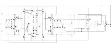
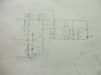
Here is the VAS section of this amplifier. The next version will use a few different components but will be the same in principle. There is no reference in this bridge to GND asside from the CCS for the cascode voltage sources. The common mode is controled through the pre-amp by the 2 DC servo circuits. Also there are no mirrors, not that I have a problem with current mirrors, they are great but don't fit in this circuit. The common mode FB loops maintain a constant current in the bridge so the bias for the output stages is solid. The transistors labled 1/2 & 2/2 are SOT 563 duel transistor packages. In reality I could even use SOT 963 components but I don't see a major advantage in space saving compared to the SOT 563 and they would be more difficult to solder.....and it seems they cost more. The SOT563 mosfets could be no smaller package though, bias 2mA @ 25V for each element so 100mW total package Pd. Details in layout are important, for example thermal PCB design for the SOT 563 mosfets have a much larger copper 'pad' area for the drain pins to absorb heat from the device, not that 100mW is out of range for SOT 563, but reduces temperature change. The +/-10V sources supply bias to the HEC output circuits. Since the FB goes to the sources of the input J-fets the gates are the only impedance for the pre-amplifier output to drive. This circuit uses lag compensation. 0.5 - 1pf is not much and is in the realm of parasitics but if they are not in this circuit it will not be stable. The +/-15V sources are the rails for the pre-amp circuit.
The +/-15V sources are the rails for the pre-amp circuit.Attachments
Hi
more....
Since the last proto-type in post 66 works so well,
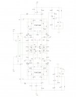
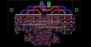
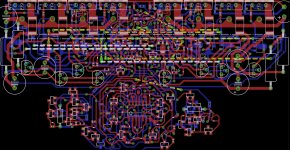
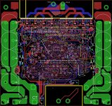
I decided to make one more build on a 2 layer PCB, but with better layout and better parts. I have yet quite a bit of work left but this is the progress so far. The output stages, most of the VAS, and most of the voltage regulator circuits are finished. The voltage regulator is series shunt, using J-fets (No Zeners ), Vin is +/-48V from a voltage doubler circuit at about 18mA. 3mA is shunted away and the circuit uses 15mA between all the pre-drivers and VAS. The voltage source for the +/-15V supply to the pre-amplifier and DC servos comes from the regulator and the 8mA of current required is sourced from the high current +/-24V VDD rails. The white dashed lines are top jumper wires and the yellow dashed lines are bottom jumper wires. The PCB above the outputs is a daughter board that will detach and and mount to the source resistors (0R1, 1W) and hold the large output current tracks. I plan to have a second daugter board to hold the speaker binding posts and output relay (if necessary). The output devices' polarity is on the same side this time for both of the seperate (optimized) HEC output stage follower circuits. The routing for these circuits is very tricky because certain tracks will contain very fast (RF) signals so good layout is critical here.
So I was doing some research into what the best way to up the power capability a bit, using the planer stripe power fets from Fairchild. I initially intended to use TO-3P size, their bigger than TO-220 so should work, eh? It turns out that TO-3P does have a larger de-rated SOA, duhhhrrr right? But, a few complications, for the same voltage amp, the Gm of the devices would be a bit low and limit the output Z, considering the high DF. In fact, the real difference between the devices is the initial heat spreader, it appears they are actually the same die. The P-ch I was going to use, FQA47P06 has been discontinued and there are no others I see available for a similar price with enough conductance. The TO-220, FQP47P06 is available, about $1.60. Looks like FQP44N10 would make a good complement, about the same cost. Two TO-220 devices has greater SOA than the TO-3P and has the conductance needed to drive a 3R speaker, so I'll go with that I suppose. Since it's two dies there is twice the input capacitance, so I beefed up the driver stage a bit. They are not exactly in paralell though, each output gate (8) has it's own dedicated class A totem pole driver, bias 25mA; split the total driver current into seperate paths so all those tiny fast, low noise, high gain small signal devices can be used and still provide adequate drive.
The output transistors will be mounted onto a thick piece of white brass, like the proto-type in post 66, but all the N-ch are mounted together and the P-ch are mounted together on just two larger seperate blocks. These blocks will be electrically insulated from the heatsink bracket and the blocks will be charged with each rail. The tabs (the drains) will be directly mounted to the blocks. There is two advantanges I see here. One is that without mica beneath each transistor, the thermal resistance is reduced between the die and the brass block increasing instantanious SOA. In addition to its thermal density, the brass block has a much larger surface area reducing thermal resistance between the block and bracket with a complete layer of mica. Second, a large thick wire can be connected to the brass block via crimp connectors and screws, keeping good isolation between the large current tracks the small signal circuitry. The drain pins are connected so that +/-Vdd can exist on the board including de-coupling. Also for the center four, the drain pin is in contact with the SOT-323 small signal device that is the EC amp and thermal compensation.
So far this is the progress, still lots of work to do. I have to add the pre-amplifier circuit along with clipping and DC detection, rectifiers, filter caps ect.
Then of course there is the review process.... .....may take some time.
BTW, even though the SMD parts are so small, none of them will ever see beyond 60% of rated Pd, most are less than 30% and many are only uW.....soldering 0201 resistors takes a steady hand........but it's not that hard.

more....
Since the last proto-type in post 66 works so well,
I decided to make one more build on a 2 layer PCB, but with better layout and better parts. I have yet quite a bit of work left but this is the progress so far. The output stages, most of the VAS, and most of the voltage regulator circuits are finished. The voltage regulator is series shunt, using J-fets (No Zeners
), Vin is +/-48V from a voltage doubler circuit at about 18mA. 3mA is shunted away and the circuit uses 15mA between all the pre-drivers and VAS. The voltage source for the +/-15V supply to the pre-amplifier and DC servos comes from the regulator and the 8mA of current required is sourced from the high current +/-24V VDD rails. The white dashed lines are top jumper wires and the yellow dashed lines are bottom jumper wires. The PCB above the outputs is a daughter board that will detach and and mount to the source resistors (0R1, 1W) and hold the large output current tracks. I plan to have a second daugter board to hold the speaker binding posts and output relay (if necessary). The output devices' polarity is on the same side this time for both of the seperate (optimized) HEC output stage follower circuits. The routing for these circuits is very tricky because certain tracks will contain very fast (RF) signals so good layout is critical here. So I was doing some research into what the best way to up the power capability a bit, using the planer stripe power fets from Fairchild. I initially intended to use TO-3P size, their bigger than TO-220 so should work, eh? It turns out that TO-3P does have a larger de-rated SOA, duhhhrrr right? But, a few complications, for the same voltage amp, the Gm of the devices would be a bit low and limit the output Z, considering the high DF. In fact, the real difference between the devices is the initial heat spreader, it appears they are actually the same die. The P-ch I was going to use, FQA47P06 has been discontinued
and there are no others I see available for a similar price with enough conductance. The TO-220, FQP47P06 is available, about $1.60. Looks like FQP44N10 would make a good complement, about the same cost. Two TO-220 devices has greater SOA than the TO-3P and has the conductance needed to drive a 3R speaker, so I'll go with that I suppose. Since it's two dies there is twice the input capacitance, so I beefed up the driver stage a bit. They are not exactly in paralell though, each output gate (8) has it's own dedicated class A totem pole driver, bias 25mA; split the total driver current into seperate paths so all those tiny fast, low noise, high gain small signal devices can be used and still provide adequate drive. The output transistors will be mounted onto a thick piece of white brass, like the proto-type in post 66, but all the N-ch are mounted together and the P-ch are mounted together on just two larger seperate blocks. These blocks will be electrically insulated from the heatsink bracket and the blocks will be charged with each rail. The tabs (the drains) will be directly mounted to the blocks. There is two advantanges I see here. One is that without mica beneath each transistor, the thermal resistance is reduced between the die and the brass block increasing instantanious SOA. In addition to its thermal density, the brass block has a much larger surface area reducing thermal resistance between the block and bracket with a complete layer of mica. Second, a large thick wire can be connected to the brass block via crimp connectors and screws, keeping good isolation between the large current tracks the small signal circuitry. The drain pins are connected so that +/-Vdd can exist on the board including de-coupling. Also for the center four, the drain pin is in contact with the SOT-323 small signal device that is the EC amp and thermal compensation.
So far this is the progress, still lots of work to do. I have to add the pre-amplifier circuit along with clipping and DC detection, rectifiers, filter caps ect.
Then of course there is the review process....
.....may take some time.BTW, even though the SMD parts are so small, none of them will ever see beyond 60% of rated Pd, most are less than 30% and many are only uW.....soldering 0201 resistors takes a steady hand....
....but it's not that hard.Attachments
Last edited:
Hi CBS240, I just want to say at this point that I am interested in your project here and balanced amplifiers in general. I am currently undertaking a research and development project for uni regarding balanced power amplifiers. It is shockingly hard to find references anywhere regarding this material, in books and the internet. It'd be great to discuss some of our ideas further here or in a new thread? In particular I am interested in ways of injecting or feeding back noise and distortion from one phase to the other in order to force it to become common-mode. This is in the vein of the Pass Super-symemtry concept.
Cheers,
Hayden
Cheers,
Hayden
It is shockingly hard to find references anywhere regarding this material, in books and the internet.
I seem to have the same problem, and very little interest here in the forum.
Unfortunately I seem to be a lone pioneer.
The only difference with XLR topology is the output is full bridge with two opposing phases. The best way to make a balanced amplifier is symetry. Precision matched components help a lot as well. I'm not sure what you mean by feeding back noise and distortion form one differential side to the other. One major advantage of XLR amps is that any existing common mode noise picked up in the source wire between the two signals and GND is canceled at the output. This assumes you have a balanced input. If the input is SE and you don't like the 'sound' of transformer distortion, things become more complex. One form of unique distortion in balanced amplifers occurs when the two output signals are slightly out of symetrical phase. For example, if you use Op-amp inverting and non-inverting circuits as a phase splitter, the phase will vary between the two amplifer outputs as frequency rises because they are not the same amplifers. The same will take place if using a single common emitter stage with equal collector and emitter resistors.
The major premise of this circuit is that it uses active bias in the form of common mode feedback loops to bias the amplifier stages. Also in the pre-amp circuit, this CMFB scheme acts as a form of error correction to correct the difference between the balanced output signals when fed by a SE source by modulating the common mode bias current. In lowering CM distortion within the amplifier, it also allows for lots of open loop GBW because of the inherent bias stability, uneffected by temperature, hence the square looking 100kHZ square wave output at 2/3 power in post 66.
Symmetry
@ CBS240
Hi, you might be interested in the Symmetry in this.
If i remember correctly it followed on to the next issue or 2, with later discussions etc.
Tried to find a PDF for you but wasn't able to locate it I have the original issues, but not with me here.
If you find a good link please share it
Regards
@ CBS240
Hi, you might be interested in the Symmetry in this.
Erno Borbely, High power high quality amplifier using mosfets, Wireless World, March 1983
If i remember correctly it followed on to the next issue or 2, with later discussions etc.
Tried to find a PDF for you but wasn't able to locate it
I have the original issues, but not with me here.If you find a good link please share it
Regards
This is the most components inflated amps i ve seen in years if not ever.
Was it really necessary to have high enough perfs ??..
On a more traditionnal design, i manage easily 500khz
BW with about 26 transistors for the complete amp
with THD in the sub ppm range for voltage output
in the same order as the ones you re targeting..
Was it really necessary to have high enough perfs ??..
On a more traditionnal design, i manage easily 500khz
BW with about 26 transistors for the complete amp
with THD in the sub ppm range for voltage output
in the same order as the ones you re targeting..
- Status
- This old topic is closed. If you want to reopen this topic, contact a moderator using the "Report Post" button.
- Home
- Amplifiers
- Solid State
- My Bridge Amp