Hi Carlos
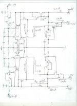
It's changed a bit since then, as I'm sure many DIY'er projects do. I don't have a good program for electronic drafting, but I think I can show the schematic in sections, since that is the way it operates anyway, to better understand this adventure into a compound circuit.") Values would be harder to read so I noted some current flows. It's hard to get the idea without a schematic. So here is another attempt...
Values would be harder to read so I noted some current flows. It's hard to get the idea without a schematic. So here is another attempt...
The voltage regulator section drives regulated DC to everything except the output transistor drains. This adds up to about 30mA. Output voltage is +/-40V, and +/-15V. It is possible to use a voltage doubler/half wave rectifier from the lower mosfet power source to drive this higher voltage. I did it this way just to see how it works. There is no hum, but of course a full wave rectifier would be better. Not counting the pass transistors, the reg circuits eat up a whole 600uA, and with no Zeners. Those J-fet's are happy at about 100uA. There are 2 matched pairs of J-fets in this stage.
It's changed a bit since then, as I'm sure many DIY'er projects do. I don't have a good program for electronic drafting, but I think I can show the schematic in sections, since that is the way it operates anyway, to better understand this adventure into a compound circuit.
Values would be harder to read so I noted some current flows. It's hard to get the idea without a schematic. So here is another attempt...The voltage regulator section drives regulated DC to everything except the output transistor drains. This adds up to about 30mA. Output voltage is +/-40V, and +/-15V. It is possible to use a voltage doubler/half wave rectifier from the lower mosfet power source to drive this higher voltage. I did it this way just to see how it works. There is no hum, but of course a full wave rectifier would be better. Not counting the pass transistors, the reg circuits eat up a whole 600uA, and with no Zeners.
Those J-fet's are happy at about 100uA. There are 2 matched pairs of J-fets in this stage.Attachments
This circuit is the DC servos and the input follower stage, along with the first gain/phase splitting stage. This circuit has 4 matched pairs of J-fet’s, 3 different types. Ahhh yes, matching fun. The servo circuits are referenced to each output separately. This is DC global feedback, but AC has no global loop. The servo circuit will bias about 3-4 VDC to each input. The DC voltage input for the +in and –in is close but not quite equal to each other, however, it will balance out to 0 VDC on each output across the speaker, and to ground. In fact the offset is never more than about 15 mV in this circuit, but it depends on Vgs matching and equal bias in the servo differentials. Using the balanced bridge as a phase splitter ensures the phase difference of the output signals is always 180 degrees, no matter what the frequency. The -3dB gain frequency points are at 18Hz or so on the low side, and around 500KHz on the high side. Even at 1MHz, the phase does not distort at the output.
The servo circuits are referenced to each output separately. This is DC global feedback, but AC has no global loop. The servo circuit will bias about 3-4 VDC to each input. The DC voltage input for the +in and –in is close but not quite equal to each other, however, it will balance out to 0 VDC on each output across the speaker, and to ground. In fact the offset is never more than about 15 mV in this circuit, but it depends on Vgs matching and equal bias in the servo differentials. Using the balanced bridge as a phase splitter ensures the phase difference of the output signals is always 180 degrees, no matter what the frequency. The -3dB gain frequency points are at 18Hz or so on the low side, and around 500KHz on the high side. Even at 1MHz, the phase does not distort at the output.Attachments
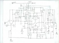
Now on to the VAS. The VAS has a local feedback loop that bias both DC and AC signals at the sources of the input J-fets. This leaves the gates floating, or rather to be driven with a DC and AC source. This is why the phase splitting circuit mismatch in output impedance is negligible, the equivalent input capacitance of these devices is about 5pf or so. Every cascade J-fet CCS in the whole circuit is set to 100uA. This makes the math simpler when figuring resistor values.
CMFB bias is employed in this stage as well as 2 THAT 340 matched arrays as the amplifying transistors in the constant power differentials. There are 3 of these arrays all together, 6 times the cost of all 4 output transistors. Still, I vouch for the THAT arrays, as I stated before, they work well for me.
The Mosfet cascode devices I don’t have yet, I am still using BJT’s, but there should be no problem there, I have used them this way once before in a previous circuit…
 …and the circuit seemed to be a little faster. Fortunately, they have the same footprint as the BJT’s so if they don’t work, the BJT will be a drop in replacement. Can’t see why they wouldn’t.
CMFB bias is employed in this stage as well as 2 THAT 340 matched arrays as the amplifying transistors in the constant power differentials. There are 3 of these arrays all together, 6 times the cost of all 4 output transistors.
Still, I vouch for the THAT arrays, as I stated before, they work well for me. The Mosfet cascode devices I don’t have yet, I am still using BJT’s, but there should be no problem there, I have used them this way once before in a previous circuit…
…and the circuit seemed to be a little faster. Fortunately, they have the same footprint as the BJT’s so if they don’t work, the BJT will be a drop in replacement. Can’t see why they wouldn’t.Attachments
Finally to the output stage. This stage should be familiar to anyone who reads this forum regularly. It works quite well. * denotes heat sink mounting. +output and –output are fed back to the servo DC detection inputs. It seems I left the output filter out, but there is an 82 Ohm resistor in series with a small 22nf polypropylene cap on each output to ground. The voltage between points A and B, C and D is about 11V.
I know this seems like a lot of trouble to get 100W RMS, but that happens sometimes when your design goals are high and you deliberately avoid using IC’s and stick to completely discrete. No real reason other than I just wanted to see if/how it could be done. This circuit should be able to use larger/parallel outputs. The operating voltage is limited by the J-fet’s in the VAS stage, but another cascode would fix all that. The capability of this circuit to be expanded is not a bad thing. Fact is, I don’t even need to listen to 100W RMS, let alone 200 or 800W. One would have to have a huge home to listen to a 800W RMS home stereo and not have reverb. Maybe this experience will help get people interested into more “No Global FB” designs. Hmmmm just dreaming, but maybe one day there could be a tracking power supply for the output drains...some day when I learn how to build one. Then again, there was a time when, to me, these results were just a transistor dream.
Ohhhh the clarity of quality audio…it’s beautiful. I can hear more detail from this circuit than any before it. The lack of noise makes classical tunes sound clear and precise. I can even understand all those background lyrics now from the music by Tool. I wish I could get more specific numbers, but I don’t have all the high tech equipment to measure every type of distortion to the N’th degree.
I know this seems like a lot of trouble to get 100W RMS, but that happens sometimes when your design goals are high and you deliberately avoid using IC’s and stick to completely discrete. No real reason other than I just wanted to see if/how it could be done. This circuit should be able to use larger/parallel outputs. The operating voltage is limited by the J-fet’s in the VAS stage, but another cascode would fix all that. The capability of this circuit to be expanded is not a bad thing. Fact is, I don’t even need to listen to 100W RMS, let alone 200 or 800W. One would have to have a huge home to listen to a 800W RMS home stereo and not have reverb.
Maybe this experience will help get people interested into more “No Global FB” designs. Hmmmm just dreaming, but maybe one day there could be a tracking power supply for the output drains...some day when I learn how to build one. Then again, there was a time when, to me, these results were just a transistor dream.Ohhhh the clarity of quality audio…it’s beautiful. I can hear more detail from this circuit than any before it. The lack of noise makes classical tunes sound clear and precise. I can even understand all those background lyrics now from the music by Tool. I wish I could get more specific numbers, but I don’t have all the high tech equipment to measure every type of distortion to the N’th degree.
Attachments
Man, you are very good...your brain is boiling with nice and hot ideas
Continue to post your ideas...people do not always make comments about our ideas... some of them feel not confortable to write posts, others want to have sure this works fine...others run to test your ideas and goes to the simulator.
We think people is not interested...sometimes we feel no one want to make it.... monthes passes and suddenlu you discover that many folks have constructed and are still listening.
There are folks that do not like to talk, to write, to advertise things, to make noises... or to show happyness.
People has some small differences..some of them are shy..others not.... and this is inside a long rule.... shy at left and not shy at rigth...many levels.
Keep the ball rolling, the machine oiled... showing us your ideas...explain them, i am sure people will read everything...if not too many people...for sure i will be reading your posts.
You know..we learn a lot with other folks solutions, ideas, problems.... this is very helpfull.... every brain storm will feed our souls with nice informs...your problem may be the solution of my doubts and may be your solution too.... keep us informed.
regards,
Carlos
I hear ya Carlos, you know I haven't run one single simulation on this circuit. It is just an expansion of other circuits I have made and those real circuits worked. This real circuit works pretty good as well but I don't know how it would work in a simulation....or if you could even fit it all in.
EDIT
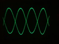
Here is 1MHz at about 3Vp per side, notice the phase is still perfectly in line with each other.
EDIT
Here is 1MHz at about 3Vp per side, notice the phase is still perfectly in line with each other.
Attachments
CBS
Oh Carlos you are too good !!!!
Oh Carlos you are too good !!!!
An externally hosted image should be here but it was not working when we last tested it.
Man!... this one remembers me a lot..we are not too much different...only in weigth..
I have 180 kg....a heavy weigth "sumo" figther..ahahahah.
Son of a whale....more to white whale than to Orca, the killer whale.
I am not so good.... but really there are folks that i really like a lot...and you are one of them Workhorse.
regards,
Carlos
....................................................................................................
Very nice wave shape CBS240
regards,
Carlos
Attachments
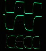
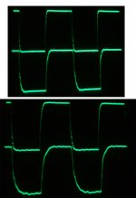
This is a 200KHz square wave, input is about 0.6V and is the top waveform. The postitive output phase is the next waveform, 10Vp per phase, at about 2A RMS. The bottom is both output waveforms. It appears better as X-axis magnification is larger in this faster signal, but both P-channel devices seem a little slow to turn on resulting in some crossover distortion. Right now, each output Mosfet gate resistor is 220 Ohms. Decreasing the gate resistor should speed up turn on, right? The signal on the gate drive is without this crossover notch. The input capacitance of the P-ch is larger than for the N-ch, they are not exactly conplementary so the resistors shouldn't have to be the same, eh? This is why I think that could be the problem. I guess I will have to test it and see.....
Right now, each output Mosfet gate resistor is 220 Ohms. Decreasing the gate resistor should speed up turn on, right? The signal on the gate drive is without this crossover notch. The input capacitance of the P-ch is larger than for the N-ch, they are not exactly conplementary so the resistors shouldn't have to be the same, eh? This is why I think that could be the problem. I guess I will have to test it and see.....Attachments
BTW, here is a 60Hz square wave, as the circuit is now, 10Vp per phase at about 2A RMS. Among all this high frequency stuff, you can't forget about the low frequency side either.
Carlos, don't you mean 180lb? You don't have the bloated face of a 396lb man.....unless you are a pro wrestler hopped up on steroids or are 7'1" like the Great Kali......and can pop a basketball or crush a man's skull with your bare hands!

Carlos, don't you mean 180lb? You don't have the bloated face of a 396lb man.....unless you are a pro wrestler hopped up on steroids
or are 7'1" like the Great Kali......and can pop a basketball or crush a man's skull with your bare hands! Attachments
180 Kilograms..... something alike 1/5 of a Ton..... may be more than 350 pounds
I think..... and i use to walk, to climb stairs and i have a new girl friend...i am 56 and she has 29....ahahahahhah.
This picture was in 99....only 320 pounds here.... today i am bigger.
Big magic my friend!
Yes... the girl is crazy...but for sure i am not.... i know how to evaluate advantages to myself.
regards,
Carlos
Attachments

Hi
As I suspected, lowering the gate resistors on the output Mosfets increased the speed and helped some with that crossover notch. I had to re-install the input wire, and twist it with a ground wire to help with the RF. The input wire was acting as an antennae and receiving RF interference from the output wire, which was in relative close proximity.
The first set of waveforms is a 100 KHz square wave, input on top, positive output on bottom. 10V @ 2A RMS, per phase. In the second set, I cranked the frequency up to 200 KHz.
Man! this circuit's fast....and very quiet too.
Attachments
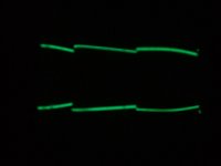
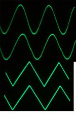
Lowering the gate resistors didn't quite compleatly get rid of the crossover problem. You can still see it in this 500KHz sine wave, but only if it is under load. Top is input, bottom is positive output phase. The negative phase looks exactly alike.
The bottom set is a 100KHz triangle wave, under load, 10Vp per phase.
The bottom set is a 100KHz triangle wave, under load, 10Vp per phase.
Attachments
Hi
An update on my quest to build the “ultimate amp”…I have had a chance to throw a few hours off at re-construction of this crazy vero-board amp prototype just to make sure that it works and was not just a fluke of physics. I have found that it works better with a slightly more compact layout, even on vero-board. This version has even less noise (better input filtering), and is faster with a bit wider bandwidth. The beauty of this latest circuit is that it can be driven with a single line input OR a balanced input. All that needs done is to change the position of a simple jumper, just like you would set a HD to either slave or master, and the output to the speaker will always be balanced from either input type. Bit of an unexpected and beneficial side effect of the way the circuit works.
I’m thinking of naming this amp the NSSKA as in Not So Simple Killer Amp. It turns out that I don’t even need an output relay for this circuit. Apparently, the bridge circuit balances strait away so there is no output to the speaker until the common mode bias balance is achieved, which takes about 2 sec. Both outputs will fluctuate positive then negative with respect to ground for that 2 seconds that it takes to settle, but the speaker is bridged between the outputs and not to ground, so both speaker terminals fluctuate positive and negative for those 2 seconds together. There is simply no output until the common mode FB and DC servos bias the circuit, then there is only signal. I found this out by accident by forgetting to remove the speaker before powering it up. My first thought was ‘crap’, rather a different 4 letter word, but to my surprise, nothing happened. I sat there and turned the power on and off several times with the speaker connected without any faults. After the first second from power up, one output measures +6mVDC and the other measures +4mVDC with respect to GND. That leaves 2mVDC on the speaker. Good enough I suppose, eh? So far, this right on target with the original goals for this circuit and it might be the version I make a PCB for. Surly if I can build this thing on vero-board, a proper PCB isn’t out of the question. Ecstatic isn’t quite the word to describe my emotions right now.
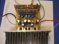
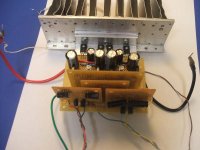
It seems I have failed to drum up much interest in non-GNFB amp designs or even symmetrical topologies. If there is one thing about this circuit, it is symmetrical, in more than one way. Really it is just separate multiple cascade symmetrical amplifiers, designed to be direct coupled with each other and to the speaker, built entirely with discrete devices, no IC’s. Talk about a trapeze balancing act. BUT it seems I have pulled it off. If there is any interest, I can try to explain how this circuit works with a bit more detail. In the mean time, here is some pictures of the construction….
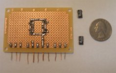
This is the start of the VAS circuit board "IC". Notice the two SOIC 14 THAT 340 matched arrays.
An update on my quest to build the “ultimate amp”…I have had a chance to throw a few hours off at re-construction of this crazy vero-board amp prototype just to make sure that it works and was not just a fluke of physics. I have found that it works better with a slightly more compact layout, even on vero-board. This version has even less noise (better input filtering), and is faster with a bit wider bandwidth. The beauty of this latest circuit is that it can be driven with a single line input OR a balanced input. All that needs done is to change the position of a simple jumper, just like you would set a HD to either slave or master, and the output to the speaker will always be balanced from either input type.
Bit of an unexpected and beneficial side effect of the way the circuit works. I’m thinking of naming this amp the NSSKA as in Not So Simple Killer Amp. It turns out that I don’t even need an output relay for this circuit. Apparently, the bridge circuit balances strait away so there is no output to the speaker until the common mode bias balance is achieved, which takes about 2 sec. Both outputs will fluctuate positive then negative with respect to ground for that 2 seconds that it takes to settle, but the speaker is bridged between the outputs and not to ground, so both speaker terminals fluctuate positive and negative for those 2 seconds together. There is simply no output until the common mode FB and DC servos bias the circuit, then there is only signal. I found this out by accident by forgetting to remove the speaker before powering it up. My first thought was ‘crap’, rather a different 4 letter word, but to my surprise, nothing happened. I sat there and turned the power on and off several times with the speaker connected without any faults. After the first second from power up, one output measures +6mVDC and the other measures +4mVDC with respect to GND. That leaves 2mVDC on the speaker. Good enough I suppose, eh?
So far, this right on target with the original goals for this circuit and it might be the version I make a PCB for. Surly if I can build this thing on vero-board, a proper PCB isn’t out of the question. Ecstatic isn’t quite the word to describe my emotions right now.It seems I have failed to drum up much interest in non-GNFB amp designs or even symmetrical topologies. If there is one thing about this circuit, it is symmetrical, in more than one way. Really it is just separate multiple cascade symmetrical amplifiers, designed to be direct coupled with each other and to the speaker, built entirely with discrete devices, no IC’s. Talk about a trapeze balancing act.
BUT it seems I have pulled it off. If there is any interest, I can try to explain how this circuit works with a bit more detail. In the mean time, here is some pictures of the construction….This is the start of the VAS circuit board "IC". Notice the two SOIC 14 THAT 340 matched arrays.
Attachments
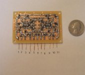
This is the finished VAS "IC".
I labeled the pins as if this circuit is a "black box"
Pin 1== -40V
Pin 2== -15V
Pin 3== +Phase output, negative bias.
Pin 4== +Phase output, positive bias.
Pin 5== +Phase input
Pin 6== GND
Pin 7== -Phase input
Pin 8== -Phase output, negative bias
Pin 9== -Phase output, positeve bias
Pin 10== +15V
Pin 11== +40V
Notice how symmetrical it looks. It is relatively easy to vero-board a symmetrical SMD circuit because the traces and wire connections are exactly alike except each complementary transistor is flipped upside down. Works great for prototyping if you can do a little solder sculpting.
Attachments
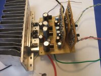
One thing is for sure though, it sure doesn't sound like it looks. Notice the 2N3904/2N3906 pair. They are the only TO-92 transistors in the circuit. I used them as the pass transistors for the voltage regulator. The entire circuit requires only 30mA from a +/- 45 to 50V supply. The output Mosfet channels are powered by a +/- 25V higher current supply. I need to dissipate up to 200mW of heat and a SOT 23 just can't quite reliably pull that off so I had to upgrade to TO-92, with some old junk parts that I refuse to throw away. See, their still good for something!
Attachments
- Status
- This old topic is closed. If you want to reopen this topic, contact a moderator using the "Report Post" button.
- Home
- Amplifiers
- Solid State
- My Bridge Amp