<snip>
I just happened to notice that just about every supply in the amp comes from a voltage doubler -- including the main B+ supply. I suggest monitoring all the supply voltages on an o'scope. I'm a little skeptical about pulling hundreds of mA from a voltage doubler, but I haven't worked that much with those. Of course, if all supplies are solid, the issue isn't with the supplies.
~Tom
Tom, you would be right to be suspicious of this. Voltage doubler is a big compromise in feeding a power stage. Look at it as a series-stacked half-wave rectified supply- as it really is.
In practice, the source impedance of the supply increases where a doubler is used. Compared to a bridge rectified supply, the voltage drop will be nearly doubled, for a step change in current demand, all else being comparable. The 18R in the rectifier feed will add to this effect. Using this supply for a high power amplifier, with high gain voltage amplifier is likely to be trouble.
doublers are OK where you have a constant current-demand, and large capacitors.
But for the power stage, I think the sound will be disappointing with a doubler, even if the instability can be fixed.
I agree, but I was concerned about the coupling between the first two stages which is where the oscillation seems to be coming from. Feedback is via the high impedance supply rail. I am concerned that the 'CCS' and the interstage coupling all have time constants in the same region of a few Hz so they will all have lots of phase shift in the same frequency region.tomchr said:I doubt it's a stability issue within the main feedback loop.
I agree with your concern about voltage doubler supplies. I had not spotted that. The last thing you need for LF stability is high impedance supply rails!
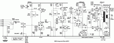
R56 to R61 are also providing some negative feedback to the B+ possibly 180 degrees out of phase to the B+ supply??? They should cancel unless they don't quite balance?
Actually no, though I can see how you reached that conclusion.
Although, it looks like R56~R61 and C31 are forming a feedback loop back to B+, they're actually just connecting from B+ to ground. C31 is just a local supply bypassing cap. I suspect R56~R61 and specifically the diodes connected in parallel with R56~R61 are to protect the OPT in case it's operated without a speaker load. That's my guess... I don't think those are part of the motor boating issue unless the amp is currently operated without speakers (or dummy load) connected.
~Tom
Last edited:
Thaks a lot for all your help, this is realy apreciated! i get some parts tomorrow and hopefully can get to test a bit more.
for now i merged the two drawings from the first post to make it easier to see the whole thing.
i detached the ccs on V2 and replaced it with a resistor for testing, there is only one ccs @V1 and the one in the LTP.
the amp is connected to a 8r resistor.
Feedback is diconnected-
the second channel 320V b+ is disconnected.
i drive it from a pc or a freq. gen, (el cheapo) no difference,
set to 40Hz. I can see a blury (looks like its there twice) wave on the oscilloscope when i measure on the cathode of the output tubes. the Led on the protection circuit flashes, my guess its about 2 Hz, as soon as the Vol. pot is turned up and the amp produces about 5V into the load of 8r.
if i detach the protection circuit from the output tubes there is no change on the oscilloscope.
@melB i shorted R1 ( was suggested before) and there was no change.
i was suspicious of the doublers as well, but the guy who designed the circuit i used mentioned that he does that all the time with success..
as i wondered in the original post, would a regulator in the b+ help with the stability of the b+ even if its positioned after a Doubler?
Attachments
i drive it from a pc or a freq. gen, (el cheapo) no difference,
set to 40Hz. I can see a blury (looks like its there twice) wave on the oscilloscope when i measure on the cathode of the output tubes.
Are there any issues when the amp is driven by other frequencies or the input is grounded (no signal)? Your most recent post seems to indicate that the problem goes away when the volume is turned down. Is this correct?
If the problem is only there during sine wave testing at very low frequencies and goes away when the signal is removed, then my bet is that you're looking at supply sag and excessive supply ripple. That would also explain why you're seeing a "double trace" on the oscilloscope. If this is the case, you should see the problem get worse at even lower input frequencies and higher input signal amplitudes.
LF sine wave testing is pretty hard on an amp. The voltage doubler supply makes this even harder as the supply caps are charged at 50 Hz not 100 Hz as they would be with a "normal" supply. The reason you're seeing the bias LEDs blink is then probably that you have the 40 Hz signal beating against the 50 Hz mains. If this is the case, I'd expect the amp to be able to reproduce 40 Hz at low output powers but not at higher output powers. Is this what you're seeing in your circuit? If that is what you're seeing in your circuit, the only solution I can think of is to increase C8, C9. Or accept that you can't reproduce <40 Hz at full output power.
Have you looked at the supply voltages with an oscilloscope yet? What were the results?
Also measure the B+ with an AC (yes AC) voltmeter. You'll probably have a few volts of AC (ripple) on the B+ with no signal. Apply 1 kHz input signal. Note the ripple voltage. Decrease the frequency. Note the change in ripple - especially below 50 Hz. What do you see?
the Led on the protection circuit flashes, my guess its about 2 Hz, as soon as the Vol. pot is turned up and the amp produces about 5V into the load of 8r.
The protection/bias monitoring circuit in Post #33 has five LEDs in it. Which one of them is flashing?
One of them is labeled "RED flashing" implying that it has a built-in circuit that makes the LED flash when power is applied (yes, that kind of LED does exist).
If the LED in series with R23 and the SCR is flashing at 2 Hz then it's because the SCR is triggered and the internal circuit in the LED is designed for 2 Hz flashing. Once the SCR has triggered the only way to turn it off is to kill its anode current. I'm guessing that's not the LED that you say is flashing as it would presumably turn off the amp via the relay marked K2.
It also looks like the diode to the right of R25 should be reversed. Otherwise that 3 second time delay won't work. Unless I'm misunderstanding something. It's a bit hard to read that schematic, honestly.
i was suspicious of the doublers as well, but the guy who designed the circuit i used mentioned that he does that all the time with success..
as i wondered in the original post, would a regulator in the b+ help with the stability of the b+ even if its positioned after a Doubler?
Doublers are often used in PC power supplies for 115 V operation. So the circuit can be designed to work. But in case of a PC, the doubler is followed by two regulators - first a power factor correction circuit (boost regulator) then the buck converter to the voltages used in the PC. Turning 115 V AC into 400 V DC and then back down to 12 V DC is a completely different story than creating a good B+ from a voltage doubler.
In your case, you should use a high-voltage regulator such as my 21st Century Maida Regulator after the doubler circuit. So the regulator input would connect to the top of C8, the regulator ground to the bottom of C9. The output of the regulator would then feed the OPTs and the rest of the power supply circuit. The regulator would reduce whatever ripple is on C8+C9 to practically nothing -- as long as the regulator always has about 20 V across it. So it wouldn't solve your issues at 40 Hz, full output power but I bet the amp would be a lot quieter and sound better with the much, much lower output impedance of the regulator.
Let's figure out what's going on with your amp before changing the supply, though.
~Tom
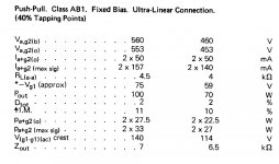
To clearly illustrate the unsuitability of voltage doublers in high-power AB1-amps, let us explore the calculations.
The output stage is KT88 class, AB1, fixed-bias, ultralinear, supply labelled 475V. This is a data-sheet condition for the KT88, and allows us to see the required demand on the power supply.
idle: 100mA [2x 50m]
full-power: 280mA [2x 140m]
We'll allow 20mA per channel for the other stages, but the exact value is not important: it is nearly constant.
The OP's schematic shows both channels hooked to the same power supply, so we must double the current demands.
The PSUD2 snap shows the outcome as the current rises from idle to full power. The degree of problems facing this design are obvious: the B+ sinks from 475V to 375V. говно! 100V sag. Even if only one channel runs from this B+, the sag will still be 70V.
The rms current in the trafo is 1,5A rms at full load, so the trafo appears to be correctly sized - but the effect of the doubler remains.
We can explore whether upgrading the quality of the doubler components might improve performance. Removing the 18R rectifier-protection resistor, and assuming that all copper-losses can be reduced to 7 ohm (referred to secondary) reduce sag to about 50V, but the rectifiers and capacitors would need to be upgraded to withstand the increased stress that this change will force.
As a calibrating remark, many guitar amps have B+ supplies that wilfully sag under load. But typical 50W Marshalls barely sag by 50V, even when played hard. To sag by 50-100V is not HiFi, for sure.
In this design, things get worse because the voltage-gain stages will suffer, when the main supplies fall. This may be enough to cause motorboating, especially if the open-loop gain of the amp is higher than necessary.
A HV Regulator will not be a good solution in this case - if we need 20V headroom (which is typical), the output voltage would need to be set to 350V, which would degrade the performance of the driver stage very badly, as 6SN7 stages like a B+ of 450V or more for a KT88-class driver. The regulator would be stressed with 125V and 30W of idle power, which would be deeply undesirable, if not absurd.
What to do?
Sharing the power supply between driver stages and power output stages is always a compromise, but with a doubler, the performance will be really bad.
The right solution depends on your expectations for the physical layout. If you can accept that a bigger power supply is needed for good performance, then I recommend that you leave the doubler supply to feed the driver and heating circuits, and use a properly specified trafo for the power stage:
primary 230V
secondary 355V with minimum 750mA rms, or 300VA rating
secondary referred resistance: 7 ohm
Bridge rectifier using UF4007 or 3A equivalents
Choke 1.3H 20 ohms DCR
Model carefully with PSUD2 to check the supply meets your design requirements.
A supply built with this, and ordinary electrolytics (Nichicon KX for preference, or LG, or Panasonic TSHA/HB or TSUP) and a 20-DCR 1.3H choke will drop only about 5V to full load and will be a platform for the best possible sound.
Such a Trafo does not need to be high cost. In most locations, industrial Panel Trafos can be bought for low cost, and here is my favourite, for UK builders:
300 VA
Whether this fixes the motorboating is not certain, but such a poor supply will make things very hard for you to debug, and even when you fix it, the performance will not be worth the effort
Attachments
The PSUD2 snap shows the outcome as the current rises from idle to full power. The degree of problems facing this design are obvious: the B+ sinks from 475V to 375V. говно! 100V sag. Even if only one channel runs from this B+, the sag will still be 70V.
Your Russian is perfect
")
Quote:
Originally Posted by Rod Coleman
The PSUD2 snap shows the outcome as the current rises from idle to full power. The degree of problems facing this design are obvious: the B+ sinks from 475V to 375V. говно! 100V sag. Even if only one channel runs from this B+, the sag will still be 70V.
Thank you for your explanations.
I agree that the doubler is not the ideal choice, yet,
if i connect both channels as it is in the circuit, and i drive one channel to clipping with a 1kHz signal the voltage drops to about 467V.
Thats quite different to the simulation...
and this is with the 18r in the circuit!
OK, but what is the idle voltage?
PSUD2 results are reliable to a good degree, but the input data must be carefully checked.
If the drop is much less than indicated, either the component values are incorrect, or the KT88s you are using do not draw the full current (and not give full output power).
Please check the component values in the PSUD2 drawing, against what you have actually used... If you can measure the trafo primary & secondary winding resistances, we can enter those accurately, too.
A measurement of rms voltage across a high-power dummy load of 8R will give us the output power too.
@Tomchr i used a zener for the reference in the ccs on V1, and there is slight improvement. i can drive the amt to produce 10V into 8r before the led starts flashing.
all the conditions are as mentioned in post 45
if i drive the amp with 1kHz there is no trouble up to clipping (17V into 8r)
there is no grid current showing on the leds, even 50Hz is fine, it starts below 40Hz.the problem gets worse when f gets smaller.
the ripple on B+, measured at the 320V rail is 20mV, same when driven with 1kHz. when i drive it with 40Hz and increse the Volume it starts to increase when the oszillations ocur. (100mV+)
the protection circuit works well, there is the scr which latches at .55V and trips the relais,this turns off the b+.
When the amp is switched of and on again, and the problem persists it trips again. the on delay works as well, just charges the caps slowly for startup and after the 3sek the resistor (in the supply circuit) is shorted out.
the other 4 leds show the grid current in the output tubes, if one draws more than 3mA it starts lightin up. one can adjust bias balance that way very easy.
whith the oszilllations its one of the two, whichever starts and if i turn up the volume a bit more the second starts flashing as well.
i wish my Test & Measurement interface for Soundcard would have a similar circuit, i just blew it when i was stupid enough to connect the wrong bnc to b+
(the measurement connector is fine with 500Vdc, the generator bnc isnt.....)
here we go more parts to be ordered, since this means my ac-voltmeter and the pc are dead for mesurements
PS its not the fault of the interface, its me !
@ Rod, the Idle of my supply with all tubes biased is 475V +- Net variation, it drops about 10V under load(clipping that is)
Last edited:
Using the circuit values in the schematic, a drop from 475v to 467V requires only a 10% increase in HT current.
If the effective anode load is far from the KT88-specified 6,5K ohm (for the other conditions) then clipping could happen well before full-power is developed - a dummy load test would confirm or deny.
Mismatched anode load will not be good for stability.
If the effective anode load is far from the KT88-specified 6,5K ohm (for the other conditions) then clipping could happen well before full-power is developed - a dummy load test would confirm or deny.
Mismatched anode load will not be good for stability.
To clearly illustrate the unsuitability of voltage doublers in high-power AB1-amps, let us explore the calculations.
idle: 100mA [2x 50m]
full-power: 280mA [2x 140m]
We'll allow 20mA per channel for the other stages, but the exact value is not important: it is nearly constant.
The OP's schematic shows both channels hooked to the same power supply, so we must double the current demands.
So... 120 mA idle, 300 mA peak per channel - or a total draw from the supply of 600 mA peak.
The PSUD2 snap shows the outcome as the current rises from idle to full power. The degree of problems facing this design are obvious: the B+ sinks from 475V to 375V. говно! 100V sag.
That's true for a step response. But the amp won't respond to DC, and probably won't see anything below 20 Hz anyway.... So I think a more reasonable test would be to use a sine wave load.
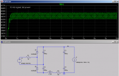
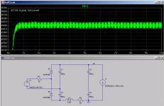
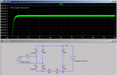
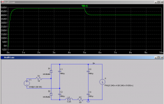
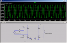
I ran a couple of quick sims in LTspice. Stare at attached. The simulation confirms Rod's result for the step response (240 mA -> 600 mA at time = 5 s), but watch as the load is changed to a sine wave. Even at 40 Hz, there's only about 6 Vpp ripple on B+. At 10 Hz this increases to 20 Vpp. At 1 kHz there's 250 mVpp ripple on B+. A regulator would reduce this ripple to practically zero.
So I don't think the supply is the problem here. It would be nice with some measurements, however. Just a simple AC voltage measurement on B+ at the different frequencies could validate my sims...
I've attached the screen shots from LTspice. The .asc file is the LTspice schematic and simulation setup if anybody's interested.
~Tom
Attachments
Er, Tom. The reason your LTspice simulations show no B+ drop is simple. You have forgotten to add a load to the modelled circuit.
Simulating a dc supply connected to a current source, without coupling it to a resistive load is equivalent to simulating a valve amplifier with the speaker disconnected.
The clue is in the data sheet. When Marconi-Osram say "Ia+Ig2, full load" they meant the dc supply current, not some ac signal.
The PSUD2 model is quite correct: the load on the dc supply rises from the idle current value (100mA per AB1 pair) to 280mA, dc values, per AB1 pair, for 70W output. The power supply must support this load, or fail.
Do the sanity-check calculation:
1. The load receives 70W.
2. dc supply ~= 500V.
3. dc current for 70W load = 70/500 = 140mA dc. Witrh the idle current & inefficiency of AB1, (~50%) there's your 280mA.
Try simulating the step from 100mA dc to 280mA dc, per channel, adding the parasitic resistances of all components, and you'll find that LTSpice agrees with Duncan, after all.
Er, Tom. The reason your LTspice simulations show no B+ drop is simple. You have forgotten to add a load to the modelled circuit.
Er, Rod... Look again. The DC load IS included. The current source on the output of the supply models the load. It's a 420 mA DC load with 360 mApp sine super-imposed on it. Stare at attached. It's a transient sim, not an AC sim.
I assumed 100 mA idle for the output stage. 20 mA constant for the input stage and phase splitter combined. 280 mA peak for the output stage. So for two channels: Idle = 2*(100 mA + 20 mA) = 240 mA. Peak = 2*(280 mA + 20 mA) = 600 mA.
The PSUD2 model is quite correct: the load on the dc supply rises from the idle current value (100mA per AB1 pair) to 280mA, dc values, per AB1 pair, for 70W output. The power supply must support this load, or fail.
As the input signal swings from zero to its maximum value, the current in one half of the output stage swings from its idle value of 100 mA to its peak value of 280 mA. As the input signals swings back down from its peak value to zero, the current in the output stage swings back to the idle value. When the signal swings negative, the current in that half of the output stage decreases. The opposite is true for the other half of the output stage as they're driven 180 degrees out of phase.
Is this not the case?
If it is the case, I would think that a push-pull stage would draw a nearly constant current. Should this not be the case, please let me know. I am mostly experienced with single-ended output stages. I don't mind being wrong as long as you back your claims up with measurements or simulations.
Try simulating the step from 100mA dc to 280mA dc, per channel, adding the parasitic resistances of all components, and you'll find that LTSpice agrees with Duncan, after all.
Did you look at my simulation schematic? It has the parasitics in there. The dominant one is the 40 ohm in series with the inductor as well as the 18 ohm in series with the secondary. My step response sim agrees pretty well with your PSUD sim. No argument there.
The current draw of the output stage, however, does not increase as a step function when you apply a signal. That would imply that the anode dissipation in the tubes jump to 140 W (70 W per anode) when you hit "PLAY" on the CD player. That's nonsensical. It would also cause rather spectacular red-plating of the output tubes. I must not be understanding you correctly.
~Tom
Attachments
Wow, this is realy taking off here. lots to learn for me.
@ Rod, i measured the winding res. of the Tranny, Rprimary= 3.1r,
Rsecondary=4.1r
you mention 70W Po, the aim of the design was 50W
@Tom, there are measurements of B+ in post#52
Quote: At 1 kHz there's 250 mVpp ripple on B+
>matches what i measured
if i understand you guys right here there are stability issues with doublers,
the sizing of the tranny is correct, would it improve stability to use 2 doublers, one for output tubes and one for input circuit
(other option would be to use one for each channel)
- Status
- This old topic is closed. If you want to reopen this topic, contact a moderator using the "Report Post" button.
- Home
- Amplifiers
- Tubes / Valves
- My amp is motorboating, improve it with b+ regulator ?