Hmmm.
Ok, so, as I understand it:
The only way to achieve symmetry is to actually use two amplifiers, is that something that`s common when relating to power amplifiers with balanced inputs?
I`m pretty sure I know what`s going on inside an unbalanced system, when it comes to balancing, I have absolutely no experience (I don`t know why I set so low values on the input resistors in the beginning, it`s pretty obvious they where to low).
Should I just drop the whole balancing issue, and go for unbalanced? I`m getting far better results in balanced mode after the last modifications. But it seems that the input impedance on the - input is pretty lower than the positive input...which of course makes sense.
Again, thanks for your contributions!
Re: Balanced input
Hi PanzerLord,
I think I've found a way to keep your Q25 and Q26 for the biasing of the output stage. As long as the output currents are easily within the class A region, you get the advantage of this bias method, i.e. a current increase in the upper half causes an (almost) equal current decrease in lower half, vice versa. For fixed voltage bias systems you don't get this linear behavior, but a reciprocal behavior instead: upper half current doubling gives lower half current halving, vice versa. Well, that is only the case for emitter resistors of 0 Ohm and BJT's. In practice it is between these extremes.
The circuit I have in mind acts as the original one, but if the currents are getting too large (for normal class A) it will keep the almost cut-off transistor conducting and allows the other one to deliver more current. The circuit will shift into class AB, but none of the output transistors will be completeley cut-off ever, so the amplifier is essentially non-switching, although operating in class AB for large output signals.
I keep you guessing for the moment, leaving you or
or  , but I would like to do some more simulations before posting. Hint: my circuit adds only two diodes and two resistors to your original circuit.
Steven
Steven[/i] [B] A nice mind-game: how can we extend the original Q25/26 construction to have its good properties for class A said:I`m stilll thinking about using the first solution using Q25 and Q26 as bias transistors...
Hi PanzerLord,
I think I've found a way to keep your Q25 and Q26 for the biasing of the output stage. As long as the output currents are easily within the class A region, you get the advantage of this bias method, i.e. a current increase in the upper half causes an (almost) equal current decrease in lower half, vice versa. For fixed voltage bias systems you don't get this linear behavior, but a reciprocal behavior instead: upper half current doubling gives lower half current halving, vice versa. Well, that is only the case for emitter resistors of 0 Ohm and BJT's. In practice it is between these extremes.
The circuit I have in mind acts as the original one, but if the currents are getting too large (for normal class A) it will keep the almost cut-off transistor conducting and allows the other one to deliver more current. The circuit will shift into class AB, but none of the output transistors will be completeley cut-off ever, so the amplifier is essentially non-switching, although operating in class AB for large output signals.
I keep you guessing for the moment, leaving you
or , but I would like to do some more simulations before posting. Hint: my circuit adds only two diodes and two resistors to your original circuit. Steven
After som soing some serious mind work around the balanced input issue, I`ve come to the conclusion that the only way to achieve 100% balancing is going for bridged mode.
I just doubled the cost!!
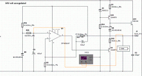
In theory, I quadrupled the power output, well I actually did it in reality also. But my main goal was to construct a 50W class A power amplifier, correct me if I`m wrong but:
-If I let the bias current be the way it is right now (total 2A per amp), the balanced (and bridged) amp will deliver 100W class A, and when the voltage swing is +14V RMS for the left one, and -14V for the right one, which gives 28V->100W in 8ohm`s; it will leave the class A mode an switch to AB when delivering 100W-200W (ok ca180W).
Look at the schematic and correct me if I`m wrong (Vcc is still the same, +/-38 for the input/VA-stage, and +/-32V for the output stage.
However in the original design I increased the input impedance so the balance was 20k/7k, I don`think I`ll construct the "bridged" design, because I honestly think there isn`t any sonic benefits when the input impedance is so much greater than the output imp of the preamp. On the other hand, if I construct my new design, my power output will be kick-!"#¤"!#!!
I just doubled the cost!!
In theory, I quadrupled the power output, well I actually did it in reality also. But my main goal was to construct a 50W class A power amplifier, correct me if I`m wrong but:
-If I let the bias current be the way it is right now (total 2A per amp), the balanced (and bridged) amp will deliver 100W class A, and when the voltage swing is +14V RMS for the left one, and -14V for the right one, which gives 28V->100W in 8ohm`s; it will leave the class A mode an switch to AB when delivering 100W-200W (ok ca180W).
Look at the schematic and correct me if I`m wrong (Vcc is still the same, +/-38 for the input/VA-stage, and +/-32V for the output stage.
However in the original design I increased the input impedance so the balance was 20k/7k, I don`think I`ll construct the "bridged" design, because I honestly think there isn`t any sonic benefits when the input impedance is so much greater than the output imp of the preamp. On the other hand, if I construct my new design, my power output will be kick-!"#¤"!#!!
Attachments
> only way to achieve 100% balancing is going for bridged mode.
No. In fact it is normally best to separate the differential-input function from the power amp function.
In your plan, if you ever must feed it an unbalanced input, you can only get 50 watts of the 200 watts you paid for.
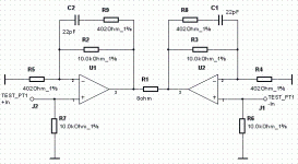
There are two main ways to take a balanced differential floating input:
The left one, without buffers, is commonly done and often better than unbalanced, but flawed. With buffers it works very well, at the cost of three separate amplifiers (though the input buffers may be unity-gain which may offer a simple solution).
The right one needs two amplifiers and has a fixed medium input impedance. It uses only inverters, which may allow a simple design or makes CMRR of an op-amp unimportant. You can't use high value resistors or noise becomes an issue. You probably don't want to try to use the power amp as the lower amp, because if you need gain (power amps usually do) then the feedback resistor value gets awful high for good stability.
There is another 2-amp diff-input which gives infinite input impedance but is confusing to gain-structure.
No. In fact it is normally best to separate the differential-input function from the power amp function.
In your plan, if you ever must feed it an unbalanced input, you can only get 50 watts of the 200 watts you paid for.
There are two main ways to take a balanced differential floating input:
An externally hosted image should be here but it was not working when we last tested it.
The left one, without buffers, is commonly done and often better than unbalanced, but flawed. With buffers it works very well, at the cost of three separate amplifiers (though the input buffers may be unity-gain which may offer a simple solution).
The right one needs two amplifiers and has a fixed medium input impedance. It uses only inverters, which may allow a simple design or makes CMRR of an op-amp unimportant. You can't use high value resistors or noise becomes an issue. You probably don't want to try to use the power amp as the lower amp, because if you need gain (power amps usually do) then the feedback resistor value gets awful high for good stability.
There is another 2-amp diff-input which gives infinite input impedance but is confusing to gain-structure.
Hmm, I think I`ll go for the original idea anyway (without buffers,as the left schematic indicated), allthough the input impedance will be unequal, I don`t think it will become a problem...adding buffer stages will add more active components in the signal path, I really don`t want to do that. I`d rather live with the impedance imbalance....
The circuit above, however, will deliver 200W (theoretically) into 8 ohm, the question is at what powerlevel...assuming the -signal is 180 degrees phasshifted related to the +signal (referred to gnd).
I not going to building an amp with option for unbalanced input, since the preamp has only balanced out.
I`ve buildt a power amp for my sub some years ago using this kind of design, and it delivered around 150W into 8ohms. I designed a phaseshifter with a inverter and a buffer...it worked nicely untill a capacitor made a hole in the ceiling (to low voltage spec.... ).
).
The circuit above, however, will deliver 200W (theoretically) into 8 ohm, the question is at what powerlevel...assuming the -signal is 180 degrees phasshifted related to the +signal (referred to gnd).
I not going to building an amp with option for unbalanced input, since the preamp has only balanced out.
I`ve buildt a power amp for my sub some years ago using this kind of design, and it delivered around 150W into 8ohms. I designed a phaseshifter with a inverter and a buffer...it worked nicely untill a capacitor made a hole in the ceiling (to low voltage spec....
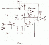
).Another way to get a balanced input and single ended output is to use a circuit with a long tail pair input, apply input signal on both bases and feedback to the emitters. Since it has a single ended output only feedback to one emitter is possible, but a resistor of equal value as the feedback resistor should be connected from the other emitter to the ground to balance the input. In this way the output will be referenced to ground. An example is the already quite old SSM2015 preamp from Solid State for Music (SSM) from the eighties. Later SSM was acquired by Analog Devices.
You can find a datasheet here.
A picture is shown below.
Don't get confused by the special biasing of the input stage by means of an additional amplifier that sets the bias curent of the input differential. This improves common mode rejection. Probably you can do without and just use current sources for the tail current.
Steven
Attachments
You see, I have a 220V to 2x23V AC transformer and a 0,3C/W heatsink laying around.
At first I wanted to design a 150-200W class AB amp, but for that I needed a 220V to 2x38V transformer. I want to put my old one in use before I do anything else.
A 0,3C/W heatsink is a bit large for a 50W class AB amp, so I thought, why not put it in real use and design a Class A instead?
The backside is, I have to buy another heatsink (ca. $80 in US currency I think).
I`m still having problems with the balancing issue, the schematic steven posted seemed logical, but that would ruin my original design (which is my first serious attempt in the upper class Hi-Fi-amps, have buildt some mid-range amps before, hence the heatsink and the tramsformer). The reason to this is, it was very important, from day one, that the design should consist of as few active components as possible in the signal path (I don`t consider the cascode as an active component in the signal path).
Adding op-amps or more gain-stages is from my point of view, undesirable, I`m actually considering going unbalanced, but we`ll see...
I Have a schematic of a matching unbalanced preamp lying around also, of course; i could drop the global NFB, but in my opinion, that is far more undesirable. This will increase THD dramtically!
I`m already working on the PCB`s, but it will take some time. This is 50% of the design process, electromagnetic influence and ground loops must be avoided at all costs
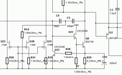
When Q10 saturates hard, when the amp goes into heavy clipping, Q9 will try to clamp the supply voltage.
Guess what happens ! Q9 will burn (yes I have seen it)
A series resistor will help Q9 survive.
What about HF stability ? Large signal stability requires more phase margin than one might think.
Good luck with testing !!
Guess what happens ! Q9 will burn (yes I have seen it)
A series resistor will help Q9 survive.
What about HF stability ? Large signal stability requires more phase margin than one might think.
Good luck with testing !!
PanzerLord said:I`m still having problems with the balancing issue, the schematic steven posted seemed logical, but that would ruin my original design (which is my first serious attempt in the upper class Hi-Fi-amps, have buildt some mid-range amps before, hence the heatsink and the tramsformer). The reason to this is, it was very important, from day one, that the design should consist of as few active components as possible in the signal path (I don`t consider the cascode as an active component in the signal path).
Adding op-amps or more gain-stages is from my point of view, undesirable, I`m actually considering going unbalanced, but we`ll see...
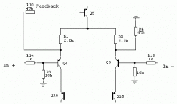
I think the concept of the SSM2015 can be incorporated in your design without adding any active component and actually leaving almost everything intact. Only the connection of the feedback should be changed and one balancing resistor added. Of course some resistor values will change. Note that now at least the input pair should be able to deal with the full input signal, because that will be applied between the input transistors, so Ic(Q5)*(R1+R2) should be big enough. This might affect the distortion in a negative way (not simulated), but that will not make the sound worse necessarily.
In the diagram I used the component labels of your first diagram in this thread.
Steven
PS I know I still have to post my Q25/26 solution.
Attachments
The input voltage on q9 will never exceed more than a few tens of millivolts, q9 and q10 is (in simple terms) a I/V converter, the "q9-stage" has a gain=<1, it acts as a buffer for the very large output impedance from the gm stage (diff amp).
So Q9 will never saturate "hard". In fact it operates in a very small area of AC voltage.
So Q9 will never saturate "hard". In fact it operates in a very small area of AC voltage.
Hi Steven, thanks for the schematic (i gotta have it on a sliver plate ), it made sense to me at once. I`ve done some simulations on it, the THD went from 0,0004% to 0.007%, nothing big, the 2nd harm went from 10uV to 400uV, and 3rd from 1uV to 100uV. These are pretty large jumps, plus, DC offset rose from -20mV to -0,7V....less CMRR?
), it made sense to me at once. I`ve done some simulations on it, the THD went from 0,0004% to 0.007%, nothing big, the 2nd harm went from 10uV to 400uV, and 3rd from 1uV to 100uV. These are pretty large jumps, plus, DC offset rose from -20mV to -0,7V....less CMRR?Distortion will go up for sure, especially the lower harmonics. You get far less loop gain, so also less feedback. This is because of the large values for R1 and R2 to make sure that the input pair can handle the complete differential input voltage. Because of less overall feedback non-linearities further on in the amplifier will also be surpressed less.
I'm a little surprised about the high offset though. Since you are simulating I would expect that you have perfect matching of the input transistors and also perfect no tolerance resistors. There seems to be a kind of unbalance around the input stage. The tail current of the differential pair is quite high compared to the base current demand of Q9, so that can hardly give an offset. Maybe you can find the cause by analysis of the simulation results. In practice the offset can be trimmed by connecting the balance resistor from Q3e not directly to ground but to a variable voltage close to ground, or even to the output of an integrator (servo) from the output, compared to ground.
Steven
Sorry, I mixed them, Gotta go to bed earlier...!
The max power capabilities for BD139 is 12,5W (ON semiconductor, not Philips which is only 8W), It can handle at 40mA at 70Vdc. I`ll of course attach it to a heatsink I think that`ll do...Im` considering placing a Re with 4-10 ohm`s for temp-stability though....and maybe...hmm..I`ll get back in a moment!
!The max power capabilities for BD139 is 12,5W (ON semiconductor, not Philips which is only 8W), It can handle at 40mA at 70Vdc. I`ll of course attach it to a heatsink I think that`ll do...Im` considering placing a Re with 4-10 ohm`s for temp-stability though....and maybe...hmm..I`ll get back in a moment!
- Status
- This old topic is closed. If you want to reopen this topic, contact a moderator using the "Report Post" button.
- Home
- Amplifiers
- Solid State
- My 50W class A design!