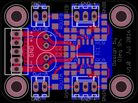
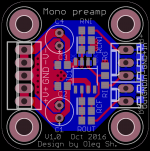
One more design idea: just turned the op-amp by 180 degrees as in the earlier design. It seems that such a position of the outputs is more convenient than in the previous post allowing for three wire stereo connection. But now the output return currents will flow all the way under the op-amp and its inputs. I guess I should not worry about it, or should I?
Regards,
Oleg
Regards,
Oleg
Attachments
Single op-amp PCB design
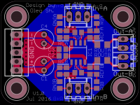
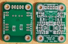
One more family member (see attached). No matter what I tried, I could not make the feedback loop shorter, only longer. I assumed that moving the feedback network to the underside of the board is not a good idea because it will interfere with the GND return of the supply currents. Does anybody have better feedback connection ideas?
The PCB is 3x3cm.
Regards,
Oleg
Attachments
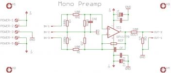
If you want to add two vias, you can put a single set of pads on the blue side (which I assume is the bottom) to fit a feedback cap from pin 6 to pin 2. This cap can go directly under the op amp, using the same center as the op amp, without any problems, and will allow some really short traces from pin 6 to pin 2 of the op amp. I'm using such an arrangement with an 0402 (1005 metric) feedback cap underneath a locally open loop 100MHz op amp and it works great - very little stray capacitance, shown by the fact that a 5pF cap there makes it stable whereas no cap is unstable.
Yes, you're cutting up the ground foil, but that cut is across the 'center line' of the foil, so it won't divert currents to bad places, or end up taking much space at all. It'd be hard to put much bigger of a cap there, but a 1005 or maybe 1608 is really all you need for stability. Then, you can remove one of the other FB pads, and allow the rest of the feedback network to wander around a little bit on the red layer without any stability problems.
The pin 6 via might get in the way of the pin 7 power trace, but there are ways to stir that around. I'll try to draw something up later to illustrate a way to fit that part into the layout.
One final thought is that using pin 8 as a 'pass-through' is slightly dangerous, since you'll have to remember to lift pin 8 for those op amps that use pin 8. Not a biggie, and not such a common problem anymore, but still something to remember when you solder in an op amp.
Hi Monte McGuire!
Thanks for the pointers! I agree that using pin 8 as pass-through is something to alway remember. I would prefer to just cut off the pin rather than lift it.
As for the feedback network placement on the underside (blue layer as you correctly guessed), I agree that it would allow for a bit shorter feedback connection and I considered such possibility as well. On the other hand doing so I would save around 5~6mm of trace length but would introduce two 1.6mm long vias (standard PCB thickness), totalling 3.2 mm. Thus the actual saving is around 2~3 mm of trace length plus the GND cut and the need to somehow reroute the power trace to pin 7. Also using packages smaller than 0805 (imperial size) is a bit impractical for an average diyer. I like soldering SMD parts but 0603 is the smallest I would ever consider and only if such a small size is absolutely necessary. I do not intend to create a PCB for MHz range applications because I'm sure I have no skill to do it properly... My main concern is audio range where I have higher chances to succeed")
Regards,
Oleg
Thanks for the pointers! I agree that using pin 8 as pass-through is something to alway remember. I would prefer to just cut off the pin rather than lift it.
As for the feedback network placement on the underside (blue layer as you correctly guessed), I agree that it would allow for a bit shorter feedback connection and I considered such possibility as well. On the other hand doing so I would save around 5~6mm of trace length but would introduce two 1.6mm long vias (standard PCB thickness), totalling 3.2 mm. Thus the actual saving is around 2~3 mm of trace length plus the GND cut and the need to somehow reroute the power trace to pin 7. Also using packages smaller than 0805 (imperial size) is a bit impractical for an average diyer. I like soldering SMD parts but 0603 is the smallest I would ever consider and only if such a small size is absolutely necessary. I do not intend to create a PCB for MHz range applications because I'm sure I have no skill to do it properly... My main concern is audio range where I have higher chances to succeed
Regards,
Oleg
Understood! I have some nice SMD tweezers, and with some nice solder paste and ideal geometry pads, you'd be surprised how well hand soldered 'tiny' SMD chips can work. I'm also doing hot air work with a stencil and an IR pre-heater, and an 01005 ESD diode actually works 100% of the time. However, without an SMD tweezer, or perhaps a pair of soldering irons, it is easy to 'tombstone' the cap, so I understand your reluctance.
The only reason I brought it up is that the vias and the traces for that feedback cap do seem to work well on the layout I've recently made, and it allows for the rest of my circuit's really wide ranging feedback path to work well with a fast op amp. My circuit is also 'just for audio', but if you want microscopic distortion, you actually want to use 50 or 100MHz op amps, just to get the feedback you need to linearize the 20kHz audio passband.
The layout looks really good now, so it's probably quite sufficient for very fast op amps. Best of luck!
I am slowly collecting various projects to submit for fabrication. Would it make sense to order thiner PCBs, e.g. 1 mm instead of standard 1.6mm? Theoretically it should provide better power decoupling and signal integrity due to smaller distance between the traces and the GND plane. I guess mechanical strength is not a problem for my PCBs since they are mostly 3x4 cm. Are there downsides that I miss?
Thanks,
Oleg
Thanks,
Oleg
Fascinating thoughts ! With 30 x 40 mm board size mechanical strength won't be a problem at all. I don't know about electrical properties like dielectric parameters that will be different... If those differences are positive or negative I can not tell but gut feeling says differences are likely to be quite marginal ( after all it is just 0,6 mm....). I hope more experienced people can you help you out on this one.
You could just try out and order one set in 1,6 mm and one in 1 mm thickness
You could just try out and order one set in 1,6 mm and one in 1 mm thickness
Last edited:
You could ask someone that has the stuff to measure it .....
There are solutions to many problems
So far I haven't considered this option
Might give it a try...The layer spacing of multilayer PCBs gets down to around 0.008" to 0.012" compared to the layer spacing of a 2layer PCB of 0.063 (1.6mm) or 0.039 (1mm)I am slowly collecting various projects to submit for fabrication. Would it make sense to order thiner PCBs, e.g. 1 mm instead of standard 1.6mm? Theoretically it should provide better power decoupling and signal integrity due to smaller distance between the traces and the GND plane. I guess mechanical strength is not a problem for my PCBs since they are mostly 3x4 cm. Are there downsides that I miss?
Thanks,
Oleg
You would still be 3 to 5 times too thick.
The benefit of close power and ground PLANES is planar capacitance, that help more at higher speed designs, for a little design like this you will get very little poser ground capacitance .so I would not worry to much about that aspect of the design, and its not worth going to 4 layers for a simple design such as this. And to get decent interplane capacitance you are looking at 0.1mm or less dialectric with basic laminate, you can go further and use special laminates that allow even better interplane capacitance, expensive. For a basic analogue design its a bit OTT.
Last edited:
Are they down to ~0.004" now?to get decent interplane capacitance you are looking at 0.1mm or less dialectric with basic laminate,
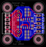
I've updated my single op-amp PCB design (attached). After warnings earlier in this thread I did not feel comfortable with the feedback signal going through the IC pad (who knows if it is really NC or offset trim input) so I routed it around and rearranged a bit the input/ground resistor on the inverting input. New trace and combined input/ground resistor pads have potentially lower parasitic capacitance to GND then the previous version which should help stability.
Regards,
Oleg
Regards,
Oleg
Attachments
- Status
- This old topic is closed. If you want to reopen this topic, contact a moderator using the "Report Post" button.
- Home
- Source & Line
- Analog Line Level
- Multi-purpose dual op-amp PCB design