Hi,
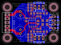
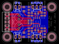
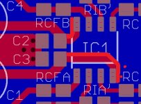
I have designed a dual op-amp PCB which allows single ended (non-inverting or inverting) and differential input connections. While the design is mostly done, what still puzzles me is the op-amp power decoupling. Attached are two variants of the PCB design. On the first variant decoupling capacitors are located next to the power pins but on the second one they are on one side of the op-amp. This second variant has approx. 4 mm extra trace length between the C3 capacitor and the negative power pin compared to the first variant. Do those 4mm matter for audio? Is it considered too far? Other than this I like the second variant more than the first one due to the more compact power input section away from the inputs. It also allows to try decoupling across the rails and not to ground.
Regards,
Oleg
PS: if you see some obvious or not so obvious problem with the design please let me know.
Attachments
Thanks for your comments, Jean-Paul!
I can move C3 to the right of the op-amp in the second version and remove the top layer copper GND pour between C1/C4. The power section would not be as nice looking as it is now but those 4 mm will be gone.
In the meantime I looked at the other designs and in the case of DIP8 packages and leaded capacitors the distances are much larger. Looking for example at Tomchr's designs with leaded capacitors at some distance from the op-amps it seems that those 4 mm should not matter much as is evident from his measurements. I guess I can now answer my own question that those extra 4 mm really do not matter much for audio performance.
Regards,
Oleg
I think the supply rail decoupling in left layout looks lower impedance.
It would be even lower if the caps C2 & C3 were placed under IC1.
Each capacitor with one pad directly under it's power pin and using 3 vias to make the top to bottom connection.
The 3 paralleled vias will add a bit of inductance (twice) but I'm pretty sure it will still be less than the long traces shown in the right layout.
This revised decoupling can be added into the space under IC1 of the right layout.
I'm not a PCB designer, but I think the vias can be closer to or even slightly overlap the pads. The copper of the via should be at the same height as the copper of the pad. Then the solder fills in the tiny gap between pin and pad/via.
Heatsink vias under a Power PAD are allowed and these could only work well if all the copper is at the same height.
Last edited:
Hi Andrew,
I think you are right that the left layout should have lower supply impedance. On the other hand the right layout has some advantages which I mentioned above.
Placing the decoupling caps on the underside of the PCB is usually discouraged in all op-amp design guides. I must say that I did not fully understand the reason for this because the in-plane loops (traces on the same side of the PCB) and the out-of-plane loops (with top to bottom layer vias) should result in similar inductance if the loop area is the same!?
Regards,
Oleg
I've got your idea now but this would introduce a via between the cap and the supply pin which is also discouraged for op-amp designs. In multiple places I read that the supply trace should first "touch" the decoupling capacitor and then continue to the supply pin. Anyways, I'll try this idea and will see what layout comes out...
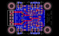
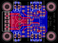
I've combined the two design ideas trying to keep the best of both (see attached). The reason for the change is that I checked the inductance of a 5 mm long trace and the value is significant. A single via has around 4 times less inductance thus using 3 vias to GND from the decoupling capacitor which is close to the power pin of the op-amp should be the way to go. I guess I'm satisfied with this PCB design version, at least for now")
Attachments
Last edited:
I just noticed that stereo three wire connection (e.g. left-GND-right) is not possible with the design above since outputs are far apart while design on the left in the first post allows this. I'm again in doubt. How frequently three wire connection is used in line level applications and are there obvious advantages/disadvantages?
Hi Oleg,
a couple of suggestions.
I've noticed that you reduce trace width from decoupling caps to opamp's pin... why?
Keeping the trace as wide as when it enters the decoupling caps pads will lower trace inductance.
I've also noticed that on the PS connector you used two pins for each rail and just one for ground return.
I would have used a 3 pin connector but using a 5 pin one I would have done exactly the opposite.
You would want the lower impedance possible for ground return.
BTW I love those triangular pads, I feel that I've seen them elsewhere... is it possible?
Hi Dario,
Thanks for looking at my designs! For me the difference in trace width is minor but I'll make it wider/equal.
The 5 pin power connector is to facilitate the sense lines connection of modern LDO regs. I just thought that it is practical and I already use it on my other designs.
Regarding the triangular pads, I haven't seen them before but you made me curious and I looked at the MyRef FE PCBs in your recent GB thread at higher magnification... and guess what? The boards I have are 1.07 version and there is just one via per R9 rathern than 3, so I couldn't see the triangles before
Thanks for looking at my designs! For me the difference in trace width is minor but I'll make it wider/equal.
The 5 pin power connector is to facilitate the sense lines connection of modern LDO regs. I just thought that it is practical and I already use it on my other designs.
Regarding the triangular pads, I haven't seen them before but you made me curious and I looked at the MyRef FE PCBs in your recent GB thread at higher magnification... and guess what?
The boards I have are 1.07 version and there is just one via per R9 rathern than 3, so I couldn't see the triangles beforeThanks for looking at my designs!
My pleasure.
For me the difference in trace width is minor but I'll make it wider/equal.
In general is better to mantain same width for the entire path, each change in width is an impedance change that could introduce unwanted reflections that could pollute your signal.
Is also true that each pad do the same so if trace widht has to be changed it is the best place to do it.
The 5 pin power connector is to facilitate the sense lines connection of modern LDO regs. I just thought that it is practical and I already use it on my other designs.
Makes sense now, thanks.
Regarding the triangular pads, I haven't seen them before but you made me curious and I looked at the MyRef FE PCBs in your recent GB thread at higher magnification... and guess what?
So we both had the same idea... interesting
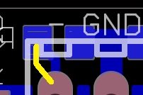
I would suggest two more things.
I would have routed those tracks from pads the other way, see the yellow line, so to keep maxim distance from the other pad.
I would consider using mitered traces so to keep reflections to the minimum.
It can be done 'automatically' selecting a radius which is around double the trace width:
In theory this should be a problem only at RF and not at audio frequencies but are we so sure that on those traces audio is the only signal present?
Attachments

Thanks for the explanation on the trace width change effect. I'll make it equal where I can. Sometimes wider trace does not fit into available space.
BTW, what is wrong with the way the trace enters the pad which you highlighted? Isn't it desired to keep the signal and its return close together?
BTW, what is wrong with the way the trace enters the pad which you highlighted? Isn't it desired to keep the signal and its return close together?
I like the original 'second' layout better, since the rectified supply currents from the bypass caps will sum more completely and will be more isolated from other components that reference ground. The trace from the ceramic cap to pin 4 of the op amp could be made electrically 'shorter' by making it wider - there's nothing going on in the red layer to prevent that, and the resulting length to width ratio will probably result in a very low impedance trace. Keep in mind that a slightly lossy dielectric like X7R will 'de-Q' the bypass and tend to minimize problems from the very slight series inductance of that trace. I think you'll win more to get the rectified signal currents to sum better than to scrape the last bit of impedance out of that pin 4 trace. They seem electrically short enough anyway, and if it's stable, then you end up getting a nice benefit with little cost.
Thanks for the explanation on the trace width change effect. I'll make it equal where I can.
You're welcome.
Sometimes wider trace does not fit into available space.
Obviously, where it's possible.
BTW, what is wrong with the way the trace enters the pad which you highlighted? Isn't it desired to keep the signal and its return close together?
Absolutely but not at the expense of reliability, that trace is too much close to ground, IMHO, and BTW we're talking about maybe 1 mm...
You could also route it a bit closer but respecting the same distance that already exists between pads.
Monte McGuire's post makes a lot of sense to me
Thanks Monte McGuire and Dario for a lot of good information!
I also liked the first version of the second layout better due to better GND routing but I could not justify the added trace impedance to pin 4. I also thought of making that trace wider but I see a drawback in possible capacitive coupling to the above chip circuitry. The wider the trace the higher this effect. I may be over engineering here but for diyer it is better this way than the other May be I should stop worrying about those anyways short traces... but chasing perfection is so much fun
I also liked the first version of the second layout better due to better GND routing but I could not justify the added trace impedance to pin 4. I also thought of making that trace wider but I see a drawback in possible capacitive coupling to the above chip circuitry. The wider the trace the higher this effect. I may be over engineering here but for diyer it is better this way than the other
May be I should stop worrying about those anyways short traces... but chasing perfection is so much funI also liked the first version of the second layout better due to better GND routing but I could not justify the added trace impedance to pin 4. I also thought of making that trace wider but I see a drawback in possible capacitive coupling to the above chip circuitry.
Simply keep it as wide as it enters the decoupling cap, something like this:
Attachments
I just calculated the inductance and capacitance of 6mm long and 1mm wide trace. The inductance is around 3nH and capacitance is around 0.4 pF. So I guess this numbers are low enough not to worry anymore and stay with the second design in the first post, just widen a bit the traces from the decoupling capacitors to the power pads of the op-amp. In TI's high speed PCB design guide the distances from the decoupling capacitor to the op-amp's power pads of less than 5 mm are considered acceptable. Here we are concerned with audio frequencies so 1 mm extra trace length should not measurably reflect on the audio performance of the op-amp, IMO. So, hopefully the final version of the PCB design is attached.
Attachments
- Status
- This old topic is closed. If you want to reopen this topic, contact a moderator using the "Report Post" button.
- Home
- Source & Line
- Analog Line Level
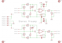
- Multi-purpose dual op-amp PCB design