Re: One more tweak here....
That is a nice pcb.
Please do not directly AC couple RXN to GND. AFAIK the reset circuit you have doubts about will do its work as it should.
Please reconsider the thought of the 3.3V and 5V regs on the pcb....
Russ White said:I adjusted some package sizes for the parts Brian has actually specked out. Thanks a ton for that hard work Brian.
Also adjusted a few cap values.
That is a nice pcb.
Please do not directly AC couple RXN to GND. AFAIK the reset circuit you have doubts about will do its work as it should.
Please reconsider the thought of the 3.3V and 5V regs on the pcb....
Re: Progress report.
Methinks you don’t understand the function of some of the DAC pins. Why would you want a pull-up/pull-down on an output? And why so many jumper options? If you consider how the circuit will be used 100% of the time you could delete most of them. Along those lines, you received some good suggestions from rfbrw, which you ignored, and you ignored the recommended layout in the datasheet. I guess you and the diyAudio Experts know more about PCB layout and component selection then the engineers who designed the chips.
Russ White said:Please, please, please take the opportunity to review things over the weekend.
Methinks you don’t understand the function of some of the DAC pins. Why would you want a pull-up/pull-down on an output? And why so many jumper options? If you consider how the circuit will be used 100% of the time you could delete most of them. Along those lines, you received some good suggestions from rfbrw, which you ignored, and you ignored the recommended layout in the datasheet. I guess you and the diyAudio Experts know more about PCB layout and component selection then the engineers who designed the chips.
Re: Re: Progress report.
Your statement about the output pin makes me wonder if you have read the data sheet yourself, though I am quite willing to concede I may have a mistake here or there... Which pin exactly are you referring to? If I have a mistake I would love for you to show me exactly how little I know, and then point me in the right direction.
The jumper options are there for flexibility.
How can I say how the circuit will be used 100% of the time? It is not just for me.... or for one purpose...
I read rfbrw suggestion very carefully. And I could not find anywhere is the CS8416 data sheet where it describes an output in regard to deemphasis .
Which part of the layout did I ignore on the data sheet? keep in mind every PCB design has some compromises. This PCB leans toward a minimum of SMT parts. So some layout considerations were necessary. Still I think I have things laid out pretty close to what is recommended.
Your last couple sentences just make you sound like you have some axe to grind. I have always plead ignorance, so you must not be talking about me.
Please be more specific if you are trying to be helpful.
Cheers!
Russ
Ulas said:
Methinks you don�t understand the function of some of the DAC pins. Why would you want a pull-up/pull-down on an output? And why so many jumper options? If you consider how the circuit will be used 100% of the time you could delete most of them. Along those lines, you received some good suggestions from rfbrw, which you ignored, and you ignored the recommended layout in the datasheet. I guess you and the diyAudio Experts know more about PCB layout and component selection then the engineers who designed the chips.
Your statement about the output pin makes me wonder if you have read the data sheet yourself, though I am quite willing to concede I may have a mistake here or there... Which pin exactly are you referring to? If I have a mistake I would love for you to show me exactly how little I know, and then point me in the right direction.
The jumper options are there for flexibility.
How can I say how the circuit will be used 100% of the time? It is not just for me.... or for one purpose...
I read rfbrw suggestion very carefully. And I could not find anywhere is the CS8416 data sheet where it describes an output in regard to deemphasis .
Which part of the layout did I ignore on the data sheet? keep in mind every PCB design has some compromises. This PCB leans toward a minimum of SMT parts. So some layout considerations were necessary. Still I think I have things laid out pretty close to what is recommended.
Your last couple sentences just make you sound like you have some axe to grind. I have always plead ignorance, so you must not be talking about me.
Please be more specific if you are trying to be helpful.
Cheers!
Russ
Re: Re: Re: Progress report.
Of course I read the datasheet: I am one of the few here who bothers with such details.
I see. So this is a commercial venture. Why do first-time DAC designers try to design a DAC for everybody else?
That wasn’t his only suggestion.
Actually, I am. You are eager to copy circuit fragments from the all-knowing diyAudio Experts but you ignore the recommendations of the chip designers. I wonder why.
It’s your design, or should I say, it’s the diyAudio Expert’s design. I am not one to tell you what to do and how to do it; there are plenty of diyAudio Experts here who think they know far more than I do and will tell you what to do and how to do it. You started this thread saying you looked at this project as a learning experience. Well, here’s your chance. Read…Think…Study…Learn. Or not.
Russ White said:Your statement about the output pin makes me wonder if you have read the data sheet yourself.
Of course I read the datasheet: I am one of the few here who bothers with such details.
Russ White said:How can I say how the circuit will be used 100% of the time? It is not just for me.... or for one purpose...
I see. So this is a commercial venture. Why do first-time DAC designers try to design a DAC for everybody else?
Russ White said:I read rfbrw suggestion very carefully. And I could not find anywhere is the CS8416 data sheet where it describes an output in regard to deemphasis.
That wasn’t his only suggestion.
Russ White said:Your last couple sentences just make you sound like you have some axe to grind. I have always plead ignorance, so you must not be talking about me.
Actually, I am. You are eager to copy circuit fragments from the all-knowing diyAudio Experts but you ignore the recommendations of the chip designers. I wonder why.
Russ White said:Please be more specific if you are trying to be helpful.
It’s your design, or should I say, it’s the diyAudio Expert’s design. I am not one to tell you what to do and how to do it; there are plenty of diyAudio Experts here who think they know far more than I do and will tell you what to do and how to do it. You started this thread saying you looked at this project as a learning experience. Well, here’s your chance. Read…Think…Study…Learn. Or not.
Ulas,
I have no idea what on earth you are are after.")
But I surely hope you find it...
I take suggestions from every place. I implement those things I can understand. I read the data sheets, and I act on them in a way that fits my project.
rfbrw made a point about possible problem if a I2S source was connected to the PCB at the same time as the receiver. I have made it clear the PCB was not designed for that (if you use external I2S you either omit the DAC or the Receiver). What other input from that person are you referring to?
I have nothing but respect for those in the forum as well as those who wrote the data sheet.
And I wish you the best friend.
:EDIT: I myself plan to use this DAC a half dozen ways... Thus the jumpers. :/EDIT:
Cheers!
Russ
I have no idea what on earth you are are after.
But I surely hope you find it...
I take suggestions from every place. I implement those things I can understand. I read the data sheets, and I act on them in a way that fits my project.
rfbrw made a point about possible problem if a I2S source was connected to the PCB at the same time as the receiver. I have made it clear the PCB was not designed for that (if you use external I2S you either omit the DAC or the Receiver). What other input from that person are you referring to?
I have nothing but respect for those in the forum as well as those who wrote the data sheet.
And I wish you the best friend.
:EDIT: I myself plan to use this DAC a half dozen ways... Thus the jumpers.
:/EDIT: Cheers!
Russ
Hi Russ,
I had a quick look at DAC's specs sheet and I saw a couple of points that could be useful.
*Wolfson recommends R of 51ohm in series for BCKIN and SCLKIN.
*output R load (R11-13-14-15) only as part of suggested external filter circuit.
Sorry if this is already known
Regards
M
I had a quick look at DAC's specs sheet and I saw a couple of points that could be useful.
*Wolfson recommends R of 51ohm in series for BCKIN and SCLKIN.
*output R load (R11-13-14-15) only as part of suggested external filter circuit.
Sorry if this is already known
Regards
M
maxlorenz said:
*Wolfson recommends R of 51ohm in series for BCKIN and SCLKIN.
*output R load (R11-13-14-15) only as part of suggested external filter circuit.
True, these series resistors are required. Output Rload resistors won't harm and can be of use with the choice of output stage. It's just good design practice to reference outputs to ground.
After the helpful comments of expert Ulas I think pins 26 and 27 of the Wolfson chip can be tied to GND continuously so no need for jumpers. The NV/ERR pin 14 can be tied low to GND by a 47K resistor. Also a LED + resistor can be connected from the pin to GND for indication of a receiver/datastream error. The same pin can be connected via an inverter/transistor to MUTEB pin 25 on the Wolfson chip as suggested by rfbrw. The MUTEB pin 25 needs to be pulled down for slow mute when an error occurs. A useful addition.
Thanks Jean-Paul
You see, even the dumb can learn...
Two questions:
*How big this R must be? 1M, 100K?
*IF I omit the output coupling cap, do I still need the R?
About output section, I understand that the Opus DAC is intended to be used "as is", wich maybe needs an active balanced preamp (DAC + Pre: one box solution?). In my case (with TVC) I will put a R in series to stay higher than 600R.
I have tried direct DAC chip outs before (AK4393) and, while being very transparent, it lacked bass omph...
Regards
M
You see, even the dumb can learn...
Output Rload resistors won't harm and can be of use with the choice of output stage.
Two questions:
*How big this R must be? 1M, 100K?
*IF I omit the output coupling cap, do I still need the R?
About output section, I understand that the Opus DAC is intended to be used "as is", wich maybe needs an active balanced preamp (DAC + Pre: one box solution?). In my case (with TVC) I will put a R in series to stay higher than 600R.
I have tried direct DAC chip outs before (AK4393) and, while being very transparent, it lacked bass omph...
Regards
M
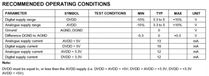
maxlorenz said:Plan to--> CDPRO-2M->direct I2S->ALW superregulated 5V (3.3V worries me
Russ White said:No worries, to do I2S in (at 5V) simply omit all the receiver related parts including the input trafo and all its associated parts.
It appears neither of you read the datasheet. What makes you think the WM8740 will work with an I2S feed from a CD transport?
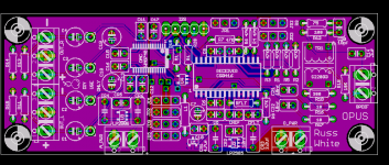
Mid weekend progress....
Ok guys (especially Jean-Paul) I hope this makes you happy.
Thanks Max, and the rest of you for you help too.
Notice the added optional VREGs(just jumper them if you don't need them) and the inverter for muting the DAC when there is a signal error. Also note the added small value resistors for the clock inputs.
Cheers!
Russ
Attachments
Dear Ulas,
No, it's true. I have not read it yet (not that I can fully understand it either). I will, as soon as I recover from my 24hrs guard...
I'll try to understand if it can accept 16bit I2S, Philips format
Dear Russ,
You're welcome we are all trying to learn here...
No, it's true. I have not read it yet (not that I can fully understand it either). I will, as soon as I recover from my 24hrs guard...
I'll try to understand if it can accept 16bit I2S, Philips format
Dear Russ,
You're welcome
we are all trying to learn here...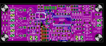
It seems I should connect the two ground planes. Maybe with a Ferrite/inductor and/or a small value resistor,
From WM8740 data sheet it appears that DGND and AGND must be at or very close to the same DC potential.
So whats the best way? A simple resistor/jumper? Or Ferrite/Inductor? Or maybe both....
From WM8740 data sheet it appears that DGND and AGND must be at or very close to the same DC potential.
So whats the best way? A simple resistor/jumper? Or Ferrite/Inductor? Or maybe both....
Attachments
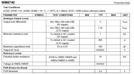
A note about the voltage output...
I have had a few questions regarding the output. The WM8740 data sheet says that it can drive a load as low as 1K, so if you have a good high impedance stage after the DAC, you should not need any buffer. Even on the evaluation board you can bypass the output op amp circuit which in that case is not really a buffer, but a filter circuit.
My planned chain is this:
DAC --> Joshua Tree attenuator(with about 4K worst case input impedance) -->Twisted Sibling balanced preamp (100K input impedance) --> Twisted X Overture balanced power amp(2.2K input impedance) --> various sundry speakers 4 and 8 ohm.
Cheers!
Russ
Attachments
- Status
- This old topic is closed. If you want to reopen this topic, contact a moderator using the "Report Post" button.
- Home
- More Vendors...
- Twisted Pear
- Mr White's "Opus", designing a simple balanced DAC