Hi Juan,
I think Mr. Miles is on holiday, when he comes back, i am sure he will reply.
reg
prasi
oh is ok I can wait
") no problem
no problem Regards
Juan
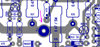
I made errata on me redrawing
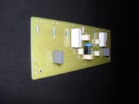
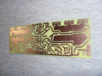
I made a mistake on the redrawing of the Apex HV23 I think will be appropriated to mention that I place that 460 ohms resistor close to the J jumper I just fixed fieuuu ! that will be really sad if I order some and that mistake is there catastrophic failure to me lol
I made a mistake on the redrawing of the Apex HV23 I think will be appropriated to mention that I place that 460 ohms resistor close to the J jumper I just fixed
fieuuu ! that will be really sad if I order some and that mistake is there catastrophic failure to me lol Attachments
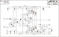
wrong post sir this is for Apex HV23 mosfet amplifier just keep Apex HV23 subjectGreetings mr.vaargas pls share aud200u amp schematic
This is class AB amplifier, bias is overcompensated and always drop when amp get warm. Amp can work in class A with lower rail voltage and large heatsink if you want.
Mr apexaudio: how many volts per rail and other details for amplifier working in class A ?. Will it improve the sound?. Thank you for your help
I made a mistake on the redrawing of the Apex HV23 I think will be appropriated to mention that I place that 460 ohms resistor close to the J jumper I just fixed
Dear vargasmongo,
Can you kindly post the circuit diagram of the Apex HV 23, which corresponds to your layout ?
--gannaji
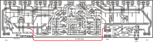
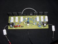
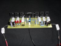
Hi Mister Mile, meanwhile I redraw your HV250, because I intend to do it. I would like to hear your opinion. Which is the maximum DC+/- voltage to run 4R, +/- 70VDC? Which value should I put on zener resistor.
Thanks in advance
Pozdrav
Thanks in advance
Pozdrav
Attachments
Hi Mister Mile, meanwhile I redraw your HV250, because I intend to do it. I would like to hear your opinion. Which is the maximum DC+/- voltage to run 4R, +/- 70VDC? Which value should I put on zener resistor.
Thanks in advance
Pozdrav
Nice work, you can use +/-70VDC without change with 4R load.
Pozdrav
Nice work, you can use +/-70VDC without change with 4R load.
Pozdrav
Thanks for your reply
Pozdrav
Hi Mister Mile, your HV250 goes slowly... I have 2 question: 1º Can I replace on positive rail NPN BD243C (65W) to 2SC4793 (20W) or MJE15032 (50W) and the same on negative rail with PNP transistors. 2º To match IRF'S I intend to use your topologi, can I use 15V insted 12V.
Thanks In advance
Pozdrav
Thanks In advance
Pozdrav
Attachments
Hi Mister Mile, your HV250 goes slowly... I have 2 question: 1º Can I replace on positive rail NPN BD243C (65W) to 2SC4793 (20W) or MJE15032 (50W) and the same on negative rail with PNP transistors. 2º To match IRF'S I intend to use your topologi, can I use 15V insted 12V.
Thanks In advance
Pozdrav
Use 2DC4793/2SA1837 and 15V is ok.
Pozdrav
Thanks for your repllyUse 2DC4793/2SA1837 and 15V is ok.
Pozdrav
apozdrav
Do not set your bias with the voltage dropping resistors in the supply lines.
Remove them after you have proved the circuit works correctly.
Use the source resistors in the output stage as your indicators of output stage bias.
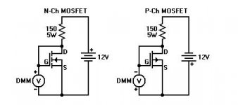
OK AndrewT, thanks for your advice. I matched the powers and how many volts should I get on source resistors. Maybe 0,023V it means 48 mA per mosfet, is it good ? I know you love calculations
Attachments

Hi Mr. Mile ! Here I am again with your HV250. At a first glance it is OK, but how many volts should a get on 10R/5W (that I put on rail +/-), in order to get a good bias. Thanks in advance.
Pozdrav
Nice work,
Pozdrav
3pair output stage equals 6 source resistors.
Set the bias voltage low to start with, maybe 10.0mVdc across Rs1 and measuure all 6 after they have reached equilibrium.
Then increase in 10.0mV increments allowing time to resettle and re-measure.
By the time you get to 50mV (100mA) you have a table of measurements for all 6 Rs
You will see if they all remain very similar, or some wander off a little, or a lot. This will really show how well you selected for Vgs.
It was a test like this that showed how much better a thin mica is at transferring heat compared to a good quality low thermal resistance soft thermal washer. I had used my last three Thermal washers for all the upper devices and reverted to mica for the opposite side.
Last edited:
It's going into my current build.
The heatsinks are all tapped and the PCB is all assembled except for the output devices.
I'm going to try measuring the open loop gain without the output devices which leaves the NFB loop open.
I plan to add one pair to the assembly for closed loop gain and initial testing.
The "Koptan" tape will be easy because I am using a 4 bolt clamping bar on each half of the 3pair output stage. The "adhesive" will be the thermal paste on one side of the tape and the Thermal Goop will be on the transistor side. No holes required in the tape!
Slight problem with the 3pair is that I am using To264 for a PCB that is spaced too tight to suit the smaller To147.
Last edited:
- Home
- Amplifiers
- Solid State
- MOSFET Amplifier IRFP240/IRFP9240