As Zeon has kindly shown you
the k170 always has the drain on the left and the source on the right.
That leaves the gate in the middle.
The j74 is the same.
There are/were only two manufacturers and both arrange the leadouts the same.
But, as with all devices look up their datasheet.
the k170 always has the drain on the left and the source on the right.
That leaves the gate in the middle.
The j74 is the same.
There are/were only two manufacturers and both arrange the leadouts the same.
But, as with all devices look up their datasheet.
As Zeon has kindly shown you
the k170 always has the drain on the left and the source on the right.
That leaves the gate in the middle.
The j74 is the same.
There are/were only two manufacturers and both arrange the leadouts the same.
But, as with all devices look up their datasheet.
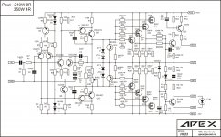
I will try one last time of explaining the problem, I hope I succeed this time. I KNOW how to find out the pinout of the devices, I also know how to read a schematic in general - what I dont know is which leg is the Drain and which is the Source (in the schematic!) posted by Apex in post #374, page 38.
I believe that the source terminals are all the ones closest to their channel's 22uF output capacitors.
 Thank you - can someone else confirm this?
This was made confusing by the nonstandard representation. The gate should be drawn closer to the source terminal than the drain on the diagram.
This was made confusing by the nonstandard representation. The gate should be drawn closer to the source terminal than the drain on the diagram.
Yes, exactly, thank you so much
")
I will draw PCB with the source terminals closest to the 22µf capacitors - hope it works. Guess I will find out the hard way
Hello mister Miles quick question, is there a jumper close to one of the 5W resistors ? I'm re-drawing and I stop right there where you see the red arrows
Regards
Juan
Regards
Juan
Attachments
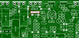
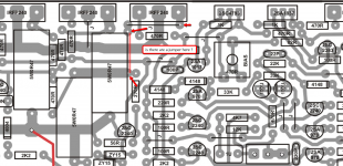
Hello mister Miles quick question, is there a jumper close to one of the 5W resistors ? I'm re-drawing and I stop right there where you see the red arrows
Regards
Juan
Yes. there is a jumper.
Regards
Hi Mile,
Can the HV23 run on 2 pairs mosfet at output?
I prefer normal listening, not high power.
What PSU and mods required?
Yes with +/-55V rail voltage
No, you aren't being stupid at all but there is a characteristic of these and many small-signal JFETs that removes the problem.....Sorry if im just stupid - but look at the picture and tell me you are not confused
Despite the fact that specific pins must be assigned to Drain and Source, 2SK/LSK 170 are among many JFETs that are completely identical in their structure and can be used either way around with impunity. I have this on the authority of wiser heads here (even John Curl now agrees) but of course, some people always become frustrated when things are not placed in a specific order, regardless of whether it matters or not.
Hello guys
I was coping again the Apex HV23 and it came out that one of the diodes D6 and R45 2K2 is not placed in the same way as the schematic is illustrated ? does some one have a problem it will work the same ? I'm trying to make it as accurate as possible
Reagards
Juan
I was coping again the Apex HV23 and it came out that one of the diodes D6 and R45 2K2 is not placed in the same way as the schematic is illustrated ? does some one have a problem it will work the same ? I'm trying to make it as accurate as possible
Reagards
Juan
Attachments

Last edited:
Hello guys
I was coping again the Apex HV23 and it came out that one of the diodes D6 and R45 2K2 is not placed in the same way as the schematic is illustrated ? does some one have a problem it will work the same ? I'm trying to make it as accurate as possible
Reagards
Juan
Parts place in series connection is irelevant.
sorry mister Miles in other words it will not matter ? I mean just to be sure
Regards
Juan
Place is no metter,
Regards
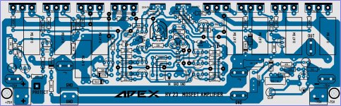
Hello mister Mile
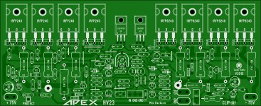
I completed the layout what you think how is it look
Regards
Juan
Nice pcb,
Regards
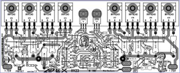
Pdf ...Pdf....PdfHello mister Mile
I completed the layout what you think how is it look
Regards
Juan
ok thimios no problem man
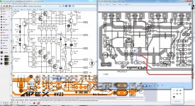
hey I also simulated today and I think I have good results not bad at all, on the software I have it does not have the transistor 2SA1033 I just place a generic one and still behave good I mean I know there are better software to simulate but at least I have an approximation sort like a percentage ok here are the files please if you notice something let me know I'm attaching the schematic I use to remake this layout I bet in real time most be sound really good
Regards
Juan
Attachments
-
Apex HV23 2015 vercion 1.1 components.pdf107.2 KB · Views: 420
-
Apex HV23 2015 vercion 1.1 hot iron transfer mirror.pdf35.5 KB · Views: 384
-
Apex HV23 2015 vercion 1.1 hot iron transfer.pdf35.4 KB · Views: 371
-
 APEX MOSFET 2SA-2SC.jpg615.8 KB · Views: 694
 -
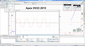 Apex HV23 2015 to 8 ohms 240W 1.3Vp sine wave 240W.PNG226.8 KB · Views: 360
 -
Apex HV23 Mosfet amplifier.pdf64.4 KB · Views: 381
- Home
- Amplifiers
- Solid State
- MOSFET Amplifier IRFP240/IRFP9240