I don't know anything about the DSD1790, but I do have experience with the current output PCM1794A. I can report after years of listening to it that passive resistor I/V can provide excellent subjective sound. While passive resistor I/V doesn't provide an ideal virtual ground node, it does exhibit nearly ideal dynamic performance, which is important at a circuit node which produces an high frequency signal and noise content.
I utilize 75 ohm I/V resistors with my PCM1794A based diy DAC. The 1794A features +/- 3.9mA full scale current output. I'm presently utilizing only one phase of the signal from each channel, in single-ended fashion. It's not necessary to accept the outputs differentially. With 75 ohm I/V I've measured 0.0022% THD from the PCM1794A. I've seen 200 ohms passive I/V resistors utilized with this DAC chip in an Audio Research tubed DAC unit.
After passive resistor I/V conversion, the resulting low signal level is easily voltage amplified by the gain stage of your choice. So, you can readily employ a tube/valve gain stage if you wish to. Judging from the resistor values shown in the schematic of the your Denon's differential op-amp based I/V stage shown above in post #11, the DSD1790 outputs about +/- 3.9mA.
Last edited:
Hi,
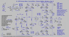
Tix, attached is a complete I/V+Buffer-stage.
The bandwidth is limited by Civ only (100kHz here), which is fully sufficient for PCM@192kHz but not for DSD (that required a 3rd order LP@50kHz iirc).
Though it may look a bit complicated at first glance, the circuit is quite simple, especially when building with matched Dual transistors.
Q1a forms a grounded base input stage which does nothing but current buffering.
Q2a is connected to Q1a to form a Sziklay-pair or CFP.
Compared to a single transistor the CFP allows for considerably lower input impedance in the mOhm range and lower THD.
It presents the DAC output a very low and constant load impedance and a high output impedance at its collector (most OPAmp-IVs fail to present a constant impedance ... and it should be low and constant up and above the output´s clock rate of the DAC, 2.84MHz iirc).
Q1b is diode connected. Its Vbe can be set by its collector current (with R2/Roffset) to the same value as Q1a´s Vbe, so that node In can be trimmed to 0mV.
As Q1a and Q1b are matched Duals here, sharing the same casing, the temperature drift is minimal.
Node In behaves like a very good ´virtual ground´.
Riv could in the simplest form be connected from Q1a´s collector to the negative supply Vn.
Unfortunately would then the PSRR be null and a DC-Offset existed at the output (Q1a´s collector) of that circuit.
So instead You find a current mirror (Q3a/Q3b/Q2b) that mirrors the DACs current into the node IV.
The current mirrors output impedance is a much better current source due to its vastly higher output impedance. Also the voltage compliance can be as high practical, or as one wishes for.
The current of the CMs output leg splits into one part going into Riv/Civ and another part flowing towards the positive supply Vp.
If the current part towards Vp is made constant and of exactly the same value as the DAC´s DC-Offset current, then only the ac signal current flows through Riv/Civ and the voltage offset over Riv/Civ would be 0.
As Riv/Civ are referenced to gnd no dc-blocking cap would then be required.
A constant current source connected between Vp and IV is required therefore.
Here I designed the CCS as current mirror (Q4a/Q5a/Q5b).
Its output leg connected to node IV and its input leg connected to J1.
J1 functions as a voltage-to-current transformer.
It´s current value depends on its gate voltage, which is connected to the output of a DC-servo (IC1).
By servo-action either the node IV or out (depending wether the servo´s input is connected to IV or out) can be made offset-free.
The rest of the circuit to the right of node IV forms a Buffer.
Q6a/Q9 and Q7a/Q10 are the heart of a cross-coupled Diamond-Buffer.
J2 is a current source that´s current is mirrored by Q12a/Q12b/Q6b resp. Q13a/Q13/Q7b into Q6a and Q7a thereby biasing the Buffer stage.
Those two current mirrors are a bit over the top, but the cost of those transistors and the required pcb area are minimal.
Due to the current mirrors the PSRR is high, reducing the burden on the quality of the supply rails.
Also the range of supply rail voltages is wider .... You can supply from +-5V up (+-9 to +-12V appear optimal).
THD-wise the I/V-circut is non-critical (around -90dB at 0dBfs) ... not bad for such a simple global feedback-free single-ended circuit.
The pic shows the design values for a PCM1795 in mono mode (-7ma +-4mA) which is close to the values of a PCM1794 in stereo mode (-6.2mA +-3.9mA).
It´d work with the PCM1794 as is, only the dc-offset at ´in´ needed a trim.
What Ken reported about the sonics of a passive Riv conversion apllies to this circuit the same, but without the need to post-amplify the signal voltage and presenting the DAC a more ´ideal´ load.
I assume in the end will both solutions be on par ... and way ahead of OPAmp equipped stages.")
jauu
Calvin
Tix, attached is a complete I/V+Buffer-stage.
The bandwidth is limited by Civ only (100kHz here), which is fully sufficient for PCM@192kHz but not for DSD (that required a 3rd order LP@50kHz iirc).
Though it may look a bit complicated at first glance, the circuit is quite simple, especially when building with matched Dual transistors.
Q1a forms a grounded base input stage which does nothing but current buffering.
Q2a is connected to Q1a to form a Sziklay-pair or CFP.
Compared to a single transistor the CFP allows for considerably lower input impedance in the mOhm range and lower THD.
It presents the DAC output a very low and constant load impedance and a high output impedance at its collector (most OPAmp-IVs fail to present a constant impedance ... and it should be low and constant up and above the output´s clock rate of the DAC, 2.84MHz iirc).
Q1b is diode connected. Its Vbe can be set by its collector current (with R2/Roffset) to the same value as Q1a´s Vbe, so that node In can be trimmed to 0mV.
As Q1a and Q1b are matched Duals here, sharing the same casing, the temperature drift is minimal.
Node In behaves like a very good ´virtual ground´.
Riv could in the simplest form be connected from Q1a´s collector to the negative supply Vn.
Unfortunately would then the PSRR be null and a DC-Offset existed at the output (Q1a´s collector) of that circuit.
So instead You find a current mirror (Q3a/Q3b/Q2b) that mirrors the DACs current into the node IV.
The current mirrors output impedance is a much better current source due to its vastly higher output impedance. Also the voltage compliance can be as high practical, or as one wishes for.
The current of the CMs output leg splits into one part going into Riv/Civ and another part flowing towards the positive supply Vp.
If the current part towards Vp is made constant and of exactly the same value as the DAC´s DC-Offset current, then only the ac signal current flows through Riv/Civ and the voltage offset over Riv/Civ would be 0.
As Riv/Civ are referenced to gnd no dc-blocking cap would then be required.
A constant current source connected between Vp and IV is required therefore.
Here I designed the CCS as current mirror (Q4a/Q5a/Q5b).
Its output leg connected to node IV and its input leg connected to J1.
J1 functions as a voltage-to-current transformer.
It´s current value depends on its gate voltage, which is connected to the output of a DC-servo (IC1).
By servo-action either the node IV or out (depending wether the servo´s input is connected to IV or out) can be made offset-free.
The rest of the circuit to the right of node IV forms a Buffer.
Q6a/Q9 and Q7a/Q10 are the heart of a cross-coupled Diamond-Buffer.
J2 is a current source that´s current is mirrored by Q12a/Q12b/Q6b resp. Q13a/Q13/Q7b into Q6a and Q7a thereby biasing the Buffer stage.
Those two current mirrors are a bit over the top, but the cost of those transistors and the required pcb area are minimal.
Due to the current mirrors the PSRR is high, reducing the burden on the quality of the supply rails.
Also the range of supply rail voltages is wider .... You can supply from +-5V up (+-9 to +-12V appear optimal).
THD-wise the I/V-circut is non-critical (around -90dB at 0dBfs) ... not bad for such a simple global feedback-free single-ended circuit.
The pic shows the design values for a PCM1795 in mono mode (-7ma +-4mA) which is close to the values of a PCM1794 in stereo mode (-6.2mA +-3.9mA).
It´d work with the PCM1794 as is, only the dc-offset at ´in´ needed a trim.
What Ken reported about the sonics of a passive Riv conversion apllies to this circuit the same, but without the need to post-amplify the signal voltage and presenting the DAC a more ´ideal´ load.
I assume in the end will both solutions be on par ... and way ahead of OPAmp equipped stages.
jauu
Calvin
Attachments
Hi,
Tix, attached is a complete I/V+Buffer-stage.
The bandwidth is limited by Civ only (100kHz here), which is fully sufficient for PCM@192kHz but not for DSD (that required a 3rd order LP@50kHz iirc).
Though it may look a bit complicated at first glance, the circuit is quite simple, especially when building with matched Dual transistors.
Q1a forms a grounded base input stage which does nothing but current buffering.
Q2a is connected to Q1a to form a Sziklay-pair or CFP.
Compared to a single transistor the CFP allows for considerably lower input impedance in the mOhm range and lower THD.
It presents the DAC output a very low and constant load impedance and a high output impedance at its collector (most OPAmp-IVs fail to present a constant impedance ... and it should be low and constant up and above the output´s clock rate of the DAC, 2.84MHz iirc).
Q1b is diode connected. Its Vbe can be set by its collector current (with R2/Roffset) to the same value as Q1a´s Vbe, so that node In can be trimmed to 0mV.
As Q1a and Q1b are matched Duals here, sharing the same casing, the temperature drift is minimal.
Node In behaves like a very good ´virtual ground´.
Riv could in the simplest form be connected from Q1a´s collector to the negative supply Vn.
Unfortunately would then the PSRR be null and a DC-Offset existed at the output (Q1a´s collector) of that circuit.
So instead You find a current mirror (Q3a/Q3b/Q2b) that mirrors the DACs current into the node IV.
The current mirrors output impedance is a much better current source due to its vastly higher output impedance. Also the voltage compliance can be as high practical, or as one wishes for.
The current of the CMs output leg splits into one part going into Riv/Civ and another part flowing towards the positive supply Vp.
If the current part towards Vp is made constant and of exactly the same value as the DAC´s DC-Offset current, then only the ac signal current flows through Riv/Civ and the voltage offset over Riv/Civ would be 0.
As Riv/Civ are referenced to gnd no dc-blocking cap would then be required.
A constant current source connected between Vp and IV is required therefore.
Here I designed the CCS as current mirror (Q4a/Q5a/Q5b).
Its output leg connected to node IV and its input leg connected to J1.
J1 functions as a voltage-to-current transformer.
It´s current value depends on its gate voltage, which is connected to the output of a DC-servo (IC1).
By servo-action either the node IV or out (depending wether the servo´s input is connected to IV or out) can be made offset-free.
The rest of the circuit to the right of node IV forms a Buffer.
Q6a/Q9 and Q7a/Q10 are the heart of a cross-coupled Diamond-Buffer.
J2 is a current source that´s current is mirrored by Q12a/Q12b/Q6b resp. Q13a/Q13/Q7b into Q6a and Q7a thereby biasing the Buffer stage.
Those two current mirrors are a bit over the top, but the cost of those transistors and the required pcb area are minimal.
Due to the current mirrors the PSRR is high, reducing the burden on the quality of the supply rails.
Also the range of supply rail voltages is wider .... You can supply from +-5V up (+-9 to +-12V appear optimal).
THD-wise the I/V-circut is non-critical (around -90dB at 0dBfs) ... not bad for such a simple global feedback-free single-ended circuit.
The pic shows the design values for a PCM1795 in mono mode (-7ma +-4mA) which is close to the values of a PCM1794 in stereo mode (-6.2mA +-3.9mA).
It´d work with the PCM1794 as is, only the dc-offset at ´in´ needed a trim.
What Ken reported about the sonics of a passive Riv conversion apllies to this circuit the same, but without the need to post-amplify the signal voltage and presenting the DAC a more ´ideal´ load.
I assume in the end will both solutions be on par ... and way ahead of OPAmp equipped stages.
jauu
Calvin
Thanks for the answer Calvin. As I understand, the DSD1790 is a difficult dac to be changed simply. The idea of Ken is the most simple, given that with the resistors will quickly minimizes the circuit. Your circuit intrigues me a lot, since it has everything already on board, and from what I understand it would be easy to modify for my dac. You have developed the pcb of your circuit?
Hi,
nope, there's no pcb.
The circuit is a beefed-up varant of a simpler proven existing design (without the CMs, Riv between Q1s collector and Vn, ac coupling via cap, cascoded JFET output buffer).
If You use the suggested Dual transisors the Layout shouldn't be very difficult.
jauu
Calvin
nope, there's no pcb.
The circuit is a beefed-up varant of a simpler proven existing design (without the CMs, Riv between Q1s collector and Vn, ac coupling via cap, cascoded JFET output buffer).
If You use the suggested Dual transisors the Layout shouldn't be very difficult.
jauu
Calvin

- Status
- This old topic is closed. If you want to reopen this topic, contact a moderator using the "Report Post" button.
- Home
- Amplifiers
- Pass Labs
- Mod denon with zen I/V