Reply
hI UPUPA EPOPS,
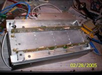
the screws you see are not for mounting purposes they are for mounting driver trannies.
Instead we use 4 screw mounted to the base plate for proper tightening.
regards,
kanwar
Upupa Epops said:You must use more screws ( one between each pair transistors ) - on other case ones in middle will be fitted wrong.
hI UPUPA EPOPS,
the screws you see are not for mounting purposes they are for mounting driver trannies.
Instead we use 4 screw mounted to the base plate for proper tightening.
regards,
kanwar
Attachments
Eva said:I don't know the purpose of these prominences [lines, points, etc..] but TO-3 devices also have them
Note that the thick heat spreading copper coin is designed to use as much surface as possible
The effect a broken base bonding wire can have on a person !
The shape of the copper coin i suppose is for easy placement on the case bottom during manufacture.
Those lines should improve soldering the die on the coin, a rough surface makes the die stick better(my guess)
Probable that those lines are created when the coin is pressed to the case bottom, i suppose pointwelding is used.
to Eva: is it real that TO-3 metal case can be made of steel??
If it is of steel, that's another pair of shoes... steel has heat conductance about three times worse than copper
I never suspected such thing - because I know for sure that old Soviet TO-3 cans where made of copper, with maybe minor adding of other metals to help make them rigid
If it is of steel, that's another pair of shoes... steel has heat conductance about three times worse than copper
I never suspected such thing - because I know for sure that old Soviet TO-3 cans where made of copper, with maybe minor adding of other metals to help make them rigid
Most of the TO-3 cases I've seen were made of steel but I've seen also some made of aluminum
Steel cases came from manufacturers like the old RCA, Motorola, National and SGS-Thomson and are the ones currently being manufactured
Aluminum cases were from Hitachi and Toshiba, but these devices are discontinued since a long ago
This explains why the bigger contact surface of TO-3 does not improve Rth-jc
The lines on the surface the die is attached to are there to prevent trapped air voids under the die. They cause hotspots.
The copper spreader's thickness causes the amount of steel case actually used for vertical heat transfer to be increased..if you make the spreader 100 mils thicker, the footprint of steel used for vertical conduction increases 200 mils in both directions. The old 45 degree spreading model..
The plastic encapsulation is not the direct limitation of the die operating temperature, it is the stability of the gain across the die as a result of diffusion and thermal transport variations. And, if inadequate base spreading or emitter bonding is present, that will limit it also..
The collector tab on a plastic device is usually a one piece stamping, from the tab, through the body, and out to the collector or drain lead on the other end.
Cheers, John
There's good practical description for heatsinking and thermal issues
http://sound.westhost.com/heatsinks.htm
http://sound.westhost.com/heatsinks.htm
jneutron said:The lines on the surface the die is attached to are there to prevent trapped air voids under the die.
The plastic encapsulation is not the direct limitation of the die operating temperature, it is the stability of the gain across the die as a result of diffusion and thermal transport variations.
The collector tab on a plastic device is usually a one piece stamping, from the tab, through the body, and out to the collector or drain lead on the other end.
John,
is the spreading of the lines on the copper coin enough to avoid any air trapped under the die, you think ?
Any idea what the minimum air void diameter can be ?
Can you tell why there are variations in thermal transport with plastic devices, i do not quite get the duffusion part ?
A one piece collector tab stamping means the collector lead is an integral part of the sink? I opened a TO247, it looked as if the collector lead was pressed into the collector tab on the sink, the tab had sharp edges on both sides of the lead connection.
Thanks for explaining all this,
J.
That is entirely dependent on the semi type, and it's temperature dependent characteristics, as well as how much energy density is being forced on the poor die..also, the thickness of the die. I've worked with dice from 10 mils, to about 25, and the dissipation is of course, on the top coupla microinches...so there is some spread before it reaches the backside.jacco vermeulen [/i]John said:Any idea what the minimum air void diameter can be ?
Diodes, for example, will go into thermal runaway over a void, as the substrate silicon will support horizontal current transport directly over the void, while the void will prevent thermal transport down..so the spot gets hotter, and it's VF goes down there, which sucks more current into the hotspot...poof.gone. Transistors will increase their leakage and gain over a hotspot, and again, poof..for example, a void directly under an emitter finger, near the emitter bond, will receive good current supply, so the gain will go up if hot..
There is such a thing as a cold void, that is when the hotter area makes the area consume less current. This is any device with a coefficient of the opposite polarity of a diode, for example..or the far tip of an emitter finger during Vsat operation, where a thin emitter metalization will have a current induced gradient, starving the hotspot of current, and reducing the power density there.
Originally posted by jacco vermeulen [/i]
Can you tell why there are variations in thermal transport with plastic devices, i do not quite get the duffusion part ?
The structure of the device, such as the pattern of the emitter fingers in a bipolar, the gate polysilicon of a mosfet, will all have a second order effect on the dissipation of the device. If there are insufficient emitter metalizations or wirebonds, for example, there will be a thermal gradient across the active area, essentially not all of the die will be working. For mosfets, the gate poly will form a voltage gradient during turn on and turn off, if sufficiently fast. A good example is a switching circuit...if you turn off the mosfet too fast, the area of the die closest to the gate will shutoff first, the source side will be more prone to blow up..too fast turn on, the gate side can blow. This can also be used to troubleshoot a snubber on the device...once the device has de-encapsulated itself (wear safety glasses), the crater location will help circuit analysis, if you understand the die..
Diffusion parameters will determine how sensitive the device is in operation, to a horizontal gradient..more sensitive, the more you have to assure a good die attach.
The devices I have worked with, the entire device was a one piece stamped copper assembly..ten to twenty devices in a row per stamping..all three leads already formed.. After the die's are attached, the wirebonds are planted, and then the entire batch of devices is placed into the molding fixture, the encapsulation process done... After this, another machine cuts the shorting bar between the three leads. Some manu's do the cutting before molding...and some separate the devices before molding.. If you look at some devices, you will see that there is exposed copper near the body, on all the leads. The IR 150's in my hand have those, but the device has been dipped, now all I can see is the shape..Originally posted by jacco vermeulen [/i]
A one piece collector tab stamping means the collector lead is an integral part of the sink? I opened a TO247, it looked as if the collector lead was pressed into the collector tab on the sink, the tab had sharp edges on both sides of the lead connection.
Lots of times, features are stamped into the copper parts. These features serve to help the plastic stay on the device, as the metal to plastic bond isn't that strong...and, some features are used to help keep the environment away from the device.
Originally posted by jacco vermeulen [/i]
Thanks for explaining all this,
J. [/B]
Not a problem..it's a pleasure to help.
Cheers, John
Mikett said:Quite often, I see a bar that clamps down on plastic transistors for heatsinking. Is this superior to using screws?
Yes. The screw only clamps the tab, but does not necessarily force intimate contact directly under the active device.
I just looked over the rest of this thread...figured I'd chip in some.
The ratings of a package are based on the ability of the package to remove the heat.
To calculate the thermal resistance of a device, you need to know the area of the die, the thickness of any heat spreader structure it is bonded to, the thickness of the case bottom.
The thermal resistance is specified with respect to the bottom of the device case. A very simple model, which btw, is quite accurate, is to use the 45 degree spread model..This model assumes the heat flow uses the entire dies bottom, and the cone of involvement includes all the material out and down, in a 45 degree pyramid..
Example, a 250 by 250 mil silicon die, bonded to a 40 mil thick copper heat spreader, then bonded to a 60 mil thick copper case..
The thermal resistance of the silicon is calculated using a 250 by 250 area silicon, 15 mil thick..
The solder attach, 250 by 250, and typically 2 to 3 mils thick.
The thermal resistance of the heat spreader is calc'd as a 40 mil thick piece of copper, 293 mils by 293 (the average size).
The bond from spreader to case...336 by 336 mils, 3 mils thick.
The case resistance, 399 by 399, 60 mils thick.
Now, comes the fun part..
When this device is used with a high conductivity insulator, you have to use a 460 by 460 heat contact area....this would be a well machined berillyia or alumina insulator. With this type of insulator, the actual mechanical integrity will have a large role in the device mounted characteristics.
If you use one of those polymer insulators, then the 45 degree model breaks down, and you have to treat the case more as an isothermal island...yes, heat will transfer over more surface area, but the penalty is the surface of the case will be at a higher operating temperature, net effect being higher thermal resistance, but less susceptible to mounting considerations.
Geeze, it's 5:00 here, I hope I added correctly, I'm typing kinda fast..
Cheers, John
I copied this from some posts I made a while back over at AA prop. It is an example of thermal resistance calculations..I used to have this on floppy disc from a while back, unfortunately I cannot find a 5.25 inch drive to stick it into..the CD drive doesn't seem to like it..
My origional program was an excel one, and it provided the thermal resistance as well as some TCE related structure numbers, which were useful for evaluating a structure's ability to withstand military temp cycling and power cycling..
Pardon the format, the "paste" didn't work too well..
The 45 degree model is a real nice and very close method to calculate the thermal resistance if a silicon die to heat sink..
Take a .250 square die, 15 mils thick.(I think that's about the size of an IR 250 series die).Attach it to a clad moly, 20 mils thick. Attach that to a BeO isolator, 25 mils thick. Then to an aluminum heat sink.
From the equation Tr=thickness/(area*K) (thickness and area units are inches and inches square)
The die thermal resistance is Tr=.015 / (.25 * .25 * 3.83) =.062 degrees C per watt.
Attach it to the moly. (for this example, I am neglecting the solder parameters).
At the top of the moly, the area is considered the same as the die. At the bottom, it is twice the thickness of the moly added to the die size in both directions. So, the heat path at the top of the moly is .25 by .25, while at the bottom, it is .250 plus .020 plus .020., or .290 inches wide. That is the 45 degree part of the model..It is assumed that the heat is spreading outward, bounded by a 45 degree "cone", as it were. (The actuals are far more complex than that, but this model is surprisingly accurate.)
So, the average area of the moly is the average between .290 and .250, or .270.
Calculate the Tr based on that: Tr= .020 / (.270 * .270 * 3.52)=.077
Next, the BeO:
The heat area at the top of that is .290, the bottom is .340.
Tr= .025 /( .315 * .315 * 6.3) = .039
So, for the package so far, the theta Jc is .062 + .077 + .039
or .178 degrees C per watt..
Now, the interesting part: In keeping with the model, the heat path at the bottom of the BeO is .315 inches by .315 inches. So, even though a full to-247 or to-3 package is heat sinked, the effective area used is a very small fraction of the total.
Say for example, a piece of elastomer is used, with a good thermal resistance (relatively)..say,,10% of alumina, at K= .094., thickness of 5 mils (both arbitrary numbers for example use only)
The effective area for the transmitted heat is .315 plus .0025, or .3175.
Tr= .005 / (.3175 * .3175 * .094) = .527 degrees C per watt.
This gives an effective Theta Jc of .527 plus .178, or .705 deg C per watt.
The actual thermal resistance of a die that size, like the IR type 250 die, is spec'd at .666 degrees C per watt, so this shows the model's accuracy.. It seems that IR specified the device thermal resistance while it is attached to a heat sink. The diff between BeO and moly vs a copper spreader is not that much.
Note the model does not use the overall package bottom for heat transfer through the elastomer...
Now, let's play a game..
Make the BeO .062 thick...and re-do the calcs..
at the top, it's .290. bottom, .408, average .352
Tr = .062 / (.352 * .352 * 6.3) = .0794 degrees C per watt.
Way larger than the .039 of the 25 mil thick stuff..
The package now has .062 + .077 + .079 =.218 C/W
But, look what happens at the insulator...
The effective area for transfer is now .408 by .408, so let's calc..
Tr = .005 / (.408 * .408 * .094) = .319 degrees c per watt.
total package just became .319 plus .218, or .537 degrees C per watt.
So...by increasing the thickness of the BeO, it is possible to lower the customer thermal resistance value..EVEN THOUGH the package thermal resistance for the thinner BeO was .178 C/W versus the .218 of the thicker BeO, the heat is more spread out by the thicker BeO, so in the end, the thicker one performs better when attached to the sink, .54 C/W vs .7...at 100 watts dissipation, that difference would allow the heat sink to go up an additional 16 degrees C for the same junction temperature, or almost a factor of four increase in semi lifetime for the same heatsink temp (assuming factor of 2 for every ten degrees C)
I had started example this using BeO, but actually, it most likely would have been copper instead...I got halfway through and decided not to change the numbers..But, increasing the package bottom thickness will have the same effect.
While seemingly rudimentary, this method has been sucessfully used in military hybrids for decades.
Thermal conductivity in watts/inch-deg C This is "K" in the equation.
Silver 10.84
Copper 10.20
Gold 8.06
BeO 6.30
Aluminum 5.30
Silicon 3.83 (heavily temp. dependent) the actual equation is 718/[T + 173]
Moly 3.52
Al2O3 (99%) 0.94 (alumina)
E/C 2851 0.05
(this is the epoxy type typically used for potted bridge rectifiers, and is one of the most thermally conductive ones available).
Cheers, John
- Status
- This old topic is closed. If you want to reopen this topic, contact a moderator using the "Report Post" button.
- Home
- Amplifiers
- Solid State
- metal vs plastic transistors