You guys are worrying too much, usual precautions when handling parts are plenty and more than sufficient. No need for copper wristbands or ESD-safe work places.
I never had a shot mosfet and I matched hundreds (all types, small signal and the big guys, N & P channel). The guys take 20V and that's quite some.
EDIT: same setup for verticals and laterals, for P-types swap + and - voltages (supply and ground) in comparison to N.
Ok - but did not know how sensitive and if the fets , big or small, needed special treatment not to blow off. Thanks for the setup info about the laterals.
rgds.
Gudmund
Normally they are sensitive no current needed to svitch them on or off just volts. Apparently if is cold and dry there is a better chance that there is poor conductivity between you and the ambient in which case your body build up electrostatic charges that could be of several thousand volts especially if you shuffle your feet on the carpet
Electrostatic charge is present in places like records attracting dust or your socks making fairy lights when you take them off
God fun but you end up with holy socks.
The current on those is relay relay small so nothing to worry about unless you have to handle fets and mosfets.
I have never blown one as far as I know but had few duff ones straight out of the packet…
Surely the supplier fault ...........................................................but maybe not.
So if your socks sparkle in the night don't play with your dudas
Better safe than sorry but yes?
Maybe just touch something metal like before you start
The Washing machine is one of the things that came to mind
Surely every one of our labs have one.
Ps do me a favor when qouting Mr T or me no need to paste the lot. Save same space and spare me to have to read his stuff which normaly is misquoted from test books and change is it happens to be proven wrong few of us have him in the ignore list so...
Gudmund
Normally they are sensitive no current needed to svitch them on or off just volts. Apparently if is cold and dry there is a better chance that there is poor conductivity between you and the ambient in which case your body build up electrostatic charges that could be of several thousand volts especially if you shuffle your feet on the carpet
Electrostatic charge is present in places like records attracting dust or your socks making fairy lights when you take them off
God fun but you end up with holy socks.
Maybe just touch something metal like before you start
The Washing machine is one of the things that came to mind
Surely every one of our labs have one.
Hi, Yes... I shall remember what you said and your wish.
Yesterday I tried to make the setup for the old Hitachi's and came out with Vgs different for the N and P types. At the setup I used 15V and 100R not the 56R as recommended.
As Hannes told us the bic fet gate takes 20V, and by use of 15V you should be on the very safe side and unable to harm the gate.
The Vgs messurement showed from 1,251 down to 0,990 between N and P types (may be some of the devices slightly more ...I can't remember). with 15V across the setup and 0,990V you should have 14,01V across the 100R or 140,1mA "waterflow" through the device??
The test was done without heatsink and within 10 sek...next test shall be on a proper heatsink and...say 20-30 sek. what do you say?
Rgds.
Hi Gudmund,
That's the way it is.
Just to clarify things: that's 20V between gate and source (VGS), source and drain take a lot more (see datasheet); when measuring VGS one is far below 20V.
If you really have 14V across the load, you're right, it amounts to 140mA drain current. But as I said, better stay out of the linear region, so choose a much smaller resistor, 10R or so is plenty, and allow the fet a drain source voltage of 5V or more.
You're on the right way, don't worry, just another step and you learned a lot")
Hannes
came out with Vgs different for the N and P types.
That's the way it is.
As Hannes told us the bic fet gate takes 20V, and by use of 15V you should be on the very safe side and unable to harm the gate.
Just to clarify things: that's 20V between gate and source (VGS), source and drain take a lot more (see datasheet); when measuring VGS one is far below 20V.
with 15V across the setup and 0,990V you should have 14,01V across the 100R or 140,1mA "waterflow" through the device??
If you really have 14V across the load, you're right, it amounts to 140mA drain current. But as I said, better stay out of the linear region, so choose a much smaller resistor, 10R or so is plenty, and allow the fet a drain source voltage of 5V or more.
You're on the right way, don't worry, just another step and you learned a lot
Hannes
Hi Gudmund,
Just to clarify things: that's 20V between gate and source (VGS), source and drain take a lot more (see datasheet); when measuring VGS one is far below 20V.
If you really have 14V across the load, you're right, it amounts to 140mA drain current. But as I said, better stay out of the linear region, so choose a much smaller resistor, 10R or so is plenty, and allow the fet a drain source voltage of 5V or more.
Hannes
Hi Hannes,
Ok - the 2SJ50/2sk135 takes approx. 160V .
I shall try with the 10R resistor and start with 5V - 10V and 15V and the devices on a heatsink. Would you say about 10 to 30 seconds or longer time for heating up?
May I ask...what does it mean to stay out of the linear region?..just in short!
Thanks for your support.
Gudmund
Hi Gudmund,
your obtainable level of matching is very likely to be more limited by the small number of fets that you have, waiting for perfect thermal equilibrium is already next level
Of course it doesn't cost a thing, so you might wait 5-10s just for fun.
However, keep an eye on power dissipation, running fets at 14VDS x 0.14 A~ 2W is already more than I would do without a heatsink.
Easy - if you look at drain current versus VDS-curve in the datasheet, you see there are two different regions. For a low VDS, the fet behaves like a resistor, means drain current changes proportionally to VDS-voltage (increase VDS and drain current increases too). You don't want that as any ripple on your power supply rails will cause ripple in drain current and things are no longer really stable.
Above 3 VDS or so drain current is stable like a rock and does not vary almost any with VDS - that's the saturation region going from these 3 V to whatever limit. That saturation region is also the reason that it doesn't make much difference wether you match at 15 VDS or at 40 VDS.
Hannes
your obtainable level of matching is very likely to be more limited by the small number of fets that you have, waiting for perfect thermal equilibrium is already next level
Of course it doesn't cost a thing, so you might wait 5-10s just for fun.
However, keep an eye on power dissipation, running fets at 14VDS x 0.14 A~ 2W is already more than I would do without a heatsink.
what does it mean to stay out of the linear region?
Easy - if you look at drain current versus VDS-curve in the datasheet, you see there are two different regions. For a low VDS, the fet behaves like a resistor, means drain current changes proportionally to VDS-voltage (increase VDS and drain current increases too). You don't want that as any ripple on your power supply rails will cause ripple in drain current and things are no longer really stable.
Above 3 VDS or so drain current is stable like a rock and does not vary almost any with VDS - that's the saturation region going from these 3 V to whatever limit. That saturation region is also the reason that it doesn't make much difference wether you match at 15 VDS or at 40 VDS.
Hannes
Hi Gudmund,
your obtainable level of matching is very likely to be more limited by the small number of fets that you have, waiting for perfect thermal equilibrium is already next level
Of course it doesn't cost a thing, so you might wait 5-10s just for fun.
However, keep an eye on power dissipation, running fets at 14VDS x 0.14 A~ 2W is already more than I would do without a heatsink.
Easy - if you look at drain current versus VDS-curve in the datasheet, you see there are two different regions. For a low VDS, the fet behaves like a resistor, means drain current changes proportionally to VDS-voltage (increase VDS and drain current increases too). You don't want that as any ripple on your power supply rails will cause ripple in drain current and things are no longer really stable.
Above 3 VDS or so drain current is stable like a rock and does not vary almost any with VDS - that's the saturation region going from these 3 V to whatever limit. That saturation region is also the reason that it doesn't make much difference wether you match at 15 VDS or at 40 VDS.
Hannes
Hi Hannes,
The test shall be limited to 5-10 sek. I shall stay away from second level now.
Because of all the information from you and other good hifi people here, things begins to light up.
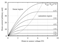
I think I found one picture which visual explains what you told me in words about staying out of the linear region and messure in the saturation region where the current does not change that much .
Please see the attached curve I found for mosfets...and this is the text below the picture:
"MOSFET drain current vs. drain-to-source voltage for several values of V G S − V t h ; the boundary between linear ( Ohmic ) and saturation ( active ) modes is indicated by the upward curving parabola."
By 5V this fets draws about, or allows a drain current of approx. 25mA.... is this correct?
The picture also explains why 5V is sufficiant for messuring (in this voltage area).
It is quite remarkable that the current is stable, "like a rock" as you said, from Vgs at only 3V? ...but one does not understand everything yet. I think to have found and read something like a slight difference in gate capacitance between the Hitachi N and P fets. Even with the best matching between N and P outputs ,it will be difficult to reach the same AC signal amplification (positive and negative sinus) because of this difference in capacitance. Is this correct?
Thanks Hannes
Attachments
Last edited:
Even with the best matching between N and P outputs ,it will be difficult to reach the same AC signal amplification (positive and negative sinus) because of this difference in capacitance. Is this correct?
Thanks Hannes
I bet the thermal coefficients are also different between N and P.
Don't worry too much about that. The main reasons to measure Vgs is first you verify that the parts are functional and second to ensure parralleled devices share the load equally. once you have that then matching between N and P is just icing on the cake.
Also if you measure Vgs at 2 current points then you can get a rough indication of transconductance of each device.
Last edited:
Hi Gudmund,
that's the exactly correct pic
No; the plot shows drain current versus VDS (drain-source) for different VGS (gate-source). In any real application the gate sees in idle never 5 VGS, it's (depending on part) between 1-2 V for laterals and 3-4 V for verticals.
So, for your lateral parts, the 2VGS curve would apply roughly. Y-axis says 'arbitrary units' - means in this case corresponding drain current is device dependent. For the big parts this current is usually already a few A or so, far above any common bias current.
For the 2 VGS curve the linear region ends at 1 VDS or so.
Real perfect matching is simply impossible as charge carrier mobility is different. Even for the same transconductance the gate capacitances will be different, so frequency responses are different (though that usually does not matter at all).
No big deal and no need to worry, really.
that's the exactly correct pic
By 5V this fets draws about, or allows a drain current of approx. 25mA.... is this correct?
No; the plot shows drain current versus VDS (drain-source) for different VGS (gate-source). In any real application the gate sees in idle never 5 VGS, it's (depending on part) between 1-2 V for laterals and 3-4 V for verticals.
So, for your lateral parts, the 2VGS curve would apply roughly. Y-axis says 'arbitrary units' - means in this case corresponding drain current is device dependent. For the big parts this current is usually already a few A or so, far above any common bias current.
For the 2 VGS curve the linear region ends at 1 VDS or so.
slight difference in gate capacitance between the Hitachi N and P fets. Even with the best matching between N and P outputs
Real perfect matching is simply impossible as charge carrier mobility is different. Even for the same transconductance the gate capacitances will be different, so frequency responses are different (though that usually does not matter at all).
No big deal and no need to worry, really.
Hi Hannes,No; the plot shows drain current versus VDS (drain-source) for different VGS (gate-source). In any real application the gate sees in idle never 5 VGS, it's (depending on part) between 1-2 V for laterals and 3-4 V for verticals.
Oh..I think I wrote things a bit wrong in english - I did not mean 5 Vgs reading..contrary I did not read the curves right -
I understood that my Vgs readings from 1,4V down to approx. 1,0V by the applied voltage of 15V was expected from laterals, and that you recommended to lower the applied voltage in the small circuit to 5V(not Vgs) and the R1 to 10 Ohm ? ( I did use 100R in the first place to reduse ampere) ...or did I get your intention wrong?
Done
...Shall do that!...and the beer!
Thanks for your patience.
Best regards
Gudmund
Use:
15V+10R+0.14 A+heatsink
be done and enjoy small beer afterwards
...Shall do that!...and the beer
! Thanks for your patience.
Best regards
Gudmund
it's not the Gate voltage you measure.
It's the Vgs that should be measured.
Now you have to decide @ what Id you want the Vgs while Vds is set to ?
and Tj=? and Tc=?
Use:
15V+10R+0.14 A+heatsink
be done and enjoy small beer afterwards
my original advice has now been followed and Ha gives you details of the final setup to test your FETs....Shall do that!...and the beer
Thanks for your patience.
Best regards
Gudmund
Every point I raised has been addressed:Tj, Tc, Id, Vds, Vgs.
Other than my writing style what was/is so wrong with my advice?
The main reasons to measure Vgs is first you verify that the parts are functional and second to ensure parralleled devices share the load equally. once you have that then matching between N and P is just icing on the cake.
Also if you measure Vgs at 2 current points then you can get a rough indication of transconductance of each device.
Thanks for the input about no need to try matching N and P types.
...and messure the Vgs at 2 current points.. to get info about the current ratio change on the output (source) leg of the fet, depending on the applied voltage changes (on the Drain)input leg.
.....I found the Shichman-Hodges model, and the transconductance for mosfets expressed as :

Mosfets and the transconductance is the change in the (drain/source) current divided by the change in the (gate/source) voltage....(as I understood) with a constant drain/source voltage.
Much more to look for...!
rgds.
Last edited:
Slow start
Hi Andrew,
No...your related terms has been answered during the communication in this thread.
"The terms" as "Tj","Tc","Id". aso....well known to you but unknown to everyone without electronic education, was mentioned on the first lines without any explaination in your first reply.
What does he think he is? ..better than the rest of the people here! could be the first thought!
A good teacher like you always starts soft with terms and words understandable for everyone. Many new electronic terms has been clearer to me during the past two weeks.
So my advice to you would be : " Take a soft start with your pupils, they are worth it".
Best regards
Gudmund
On transconductance
The folowing link posted by other member (sorry forgot your handle Qudos to you Sir)
http://technologyinterface.nmsu.edu/Fall09/Fall09/011.pdf
Still reading trough the mats but realy good writing style and explanation.
The folowing link posted by other member (sorry forgot your handle Qudos to you Sir)
http://technologyinterface.nmsu.edu/Fall09/Fall09/011.pdf
Still reading trough the mats but realy good writing style and explanation.
- Status
- This old topic is closed. If you want to reopen this topic, contact a moderator using the "Report Post" button.
- Home
- Amplifiers
- Pass Labs
- Matching Mosfets