I measured 100mV bias on 33h...
Between points A and B = 100mV ???
When measuring over the indicated points A and B, 100mV would mean 2A bias.
Even a ML33 has only 1.27A bias, or 85mA/transistor.
But when measuring from emitter to emitter 100mV would mean 1/10 of the bias current in 2x0.22R and full bias current in 2*0.025R resulting in 1.06A bias current, which is still too high , because that would mean 106mA/transistor.
Hans
Even a ML33 has only 1.27A bias, or 85mA/transistor.
But when measuring from emitter to emitter 100mV would mean 1/10 of the bias current in 2x0.22R and full bias current in 2*0.025R resulting in 1.06A bias current, which is still too high , because that would mean 106mA/transistor.
Hans
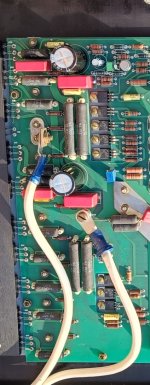
So instead of 4x0.1R in the circuit diagram, you have 2X0.33R ?Look the photo
Calculating again, this means 100mV/0,33R = 330mA or 33mA/transistor.
I would expect twice that amount.
Hans
OK, thx. i saw that classic look and didn't recognize it at all ....mlloyd1 this is a Infinity RS1B electronic crossover
Hans the resistors are 4 for side, like 331 and 336 amp.So instead of 4x0.1R in the circuit diagram, you have 2X0.33R ?
Calculating again, this means 100mV/0,33R = 330mA or 33mA/transistor.
I would expect twice that amount.
Hans
Not 0,1ohm x 4 but 0,33 x 4 for side
According to the circuit diagram it’s 8x 0.1R,
Four for the positive side and four for the negative halve.
Now on the picture of PCB I see 2x 0.33R for the positive halve and 2x 0.33R for the negative side, true ?
So 100mV between A & B is 330mA, 33mA per output transistor, as mentioned I would expect twice that amount.
Hans
Four for the positive side and four for the negative halve.
Now on the picture of PCB I see 2x 0.33R for the positive halve and 2x 0.33R for the negative side, true ?
So 100mV between A & B is 330mA, 33mA per output transistor, as mentioned I would expect twice that amount.
Hans
One side
4 x 0.33ohm NPN side / 4 x 0.33ohm PNP side . Between points A and B = 100mV .
Attachments
Hans the resistors are 4 for side, like 331 and 336 amp.
Not 0,1ohm x 4 but 0,33 x 4 for side
NO.33 is also 0.33 ohms
Yes thx, that became obvious in the previous postings
A bit odd that ML showed them in the circuit diagram as 0.1R, thereby deviating from the 0.33R in the No.33.
That raises the question how correct the other parts are in the No.33H schematic.
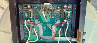
Nice pictures BTW, I’ll keep them in my archive.
Hans
One other thing becomes obvious in your images: in the No.33 description, ML talks about 3 independent groups of drivers steering 3x5 end transistors, but looking at the images, all 15 base resistors are tied together in one drive line.
That means that the 3 drivers groups are in parallel and not in individual groups.
")
A bit odd that ML showed them in the circuit diagram as 0.1R, thereby deviating from the 0.33R in the No.33.
That raises the question how correct the other parts are in the No.33H schematic.
Nice pictures BTW, I’ll keep them in my archive.
Hans
One other thing becomes obvious in your images: in the No.33 description, ML talks about 3 independent groups of drivers steering 3x5 end transistors, but looking at the images, all 15 base resistors are tied together in one drive line.
That means that the 3 drivers groups are in parallel and not in individual groups.
Last edited:
- Home
- Amplifiers
- Solid State
- Mark Levinson 33H calibration