no, not yet. the newsgroup is rec.radio.amateur.homebrew
I could always send them a small job and see how it works out. As Elso made me aware, my transistor array for the phasemeter seems to be no longer in production so I am going to have some new boards made up with an off-the-shelf high speed comparator -- perhaps I will use these guys instead of PCBExpress.
I could always send them a small job and see how it works out. As Elso made me aware, my transistor array for the phasemeter seems to be no longer in production so I am going to have some new boards made up with an off-the-shelf high speed comparator -- perhaps I will use these guys instead of PCBExpress.
Hi soundNerd,
Here is a link to toner transfer method with laser printer. The author uses it with great results.
I have not tried it myself yet but it sounds promising
Good luck
http://www.fullnet.com/u/tomg/gooteepc.htm
Here is a link to toner transfer method with laser printer. The author uses it with great results.
I have not tried it myself yet but it sounds promising
Good luck
http://www.fullnet.com/u/tomg/gooteepc.htm
thx everybody,
that paper i have still smears traces together, so I would like something that doesn't. Does that pnp stuff ever smear? can you do smd boards with it? I need to make some headphone amps with the sop version of the lm4881.
Yes it does, but only if you apply way too much pressure, probably by sitting on the iron

PNP gives extremely accurate results with very simple procedure, but they aren't cheap.
I know you're not looking for a "photo" process, but I find the positive photoresist boards very easy to work with. DSE in NZ have or at least had a green spray (aerosol) that you can paint copper with - or buy presensitised Kinsten board which is cheap enough. I have settled on using an inkjet printer (better accuracy, better contrast, very fine tracks) onto thin photo quality paper (not transparency), lining up and taping print side together against a window (for 2 sided boards). This goes in the UV exposure box (the tricky part - vaccum bag hold down and UV lamps top and bottom) for 5 minutes. Develop in solution of NaOH 5g/L lukewarm water. Etch as usual (hot ammonium persulphate in a bubble tank). I think the fastest I've done this part from print to ready to drill is 20 minutes or maybe that even included drilling (we used to have races). Drilling is the horrible part for me - I've got a DIY CNC router but it's a pain to set up. If drilling manually I like to use worn (throwaway) carbide drill bits because they self centre easier in pad holes. All hell breaks loose when you break your last drill bit on a weekend.
uhhhhh
, it's a nasty stuff!It never works and it doesn't even stick onto the board evenly!
It's a big hassle to keep the board in a dark & clean place until it dries.
The place where you dry the board must be absolutely dust free!
Sometimes it doesn't even develope, especially with the German made universal developer sold in RS components, which works really well with any other kinds of board.
Further more, the spray has very short shelf-life
It's probably the worst phtographic method that I've ever tried

That was true, until I discovered the oven: It's dark, dust free, and can dry it real quick. Plus it's in the kitchen where this stuff is best done. Drano works as developer (watch out for the new churning action bits of aluminium swarf though). My can has "USE BEFORE ????95" on it, I hope it still works.jamesjung21 said:uhhhhh
It never works and it doesn't even stick onto the board evenly!
It's a big hassle to keep the board in a dark & clean place until it dries.
The place where you dry the board must be absolutely dust free!
Sometimes it doesn't even develope, especially with the German made universal developer sold in RS components, which works really well with any other kinds of board.
Further more, the spray has very short shelf-life
It's probably the worst phtographic method that I've ever tried
Generally, it is horrible to use compared to the presensitised board which is easy and cheap. I just keep a can of this pre 1995 vintage spray handy in case I get stuck, or want to etch a nonstandard board, piece of copper, or make a screen.
The worst photographic method I ever used (indirectly) was a negative process. What a lot of muckin about. It seemed to be an endless cycle of expose-develop-expose-develop etc, the room seemed to fill up with film, wrapping and anything that can be peeled off anything else. The unweildy etch tank grumbled away for a while then the pump exploded and etchant leaked right through it. Never again!
this is my way
I work since a few weeks with the inkjet glossy paper and toner method.
Very suitable is some old HP glossy "paper", wich consists of a foil and can be removed easily when hot.
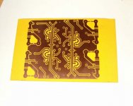
The results are not perfect, but not to bad, at all (my integrated regulated buffered stereo amp):
Before I forget it: this amps circuit is mostly based on the postings from Carlosfm. Not commercial, just for fun!
Thanks, Carlos! I am really looking forward, to listen to it.
Franz
I work since a few weeks with the inkjet glossy paper and toner method.
Very suitable is some old HP glossy "paper", wich consists of a foil and can be removed easily when hot.
The results are not perfect, but not to bad, at all (my integrated regulated buffered stereo amp):
An externally hosted image should be here but it was not working when we last tested it.
An externally hosted image should be here but it was not working when we last tested it.
Before I forget it: this amps circuit is mostly based on the postings from Carlosfm. Not commercial, just for fun!
Thanks, Carlos! I am really looking forward, to listen to it.
Franz
Re: this is my way
Just do it.
I see you intend to use trimmers.
You should use at least 1/2w resistors.
Most trimmers are too weak for this circuit, they drift, some hours later voltage will be lower. You adjust them again, and it happens again. Not the best solution. Maby with a paralleled resistor...
Franz G said:Before I forget it: this amps circuit is mostly based on the postings from Carlosfm. Not commercial, just for fun!
Thanks, Carlos! I am really looking forward, to listen to it.
Franz
Just do it.
I see you intend to use trimmers.
You should use at least 1/2w resistors.
Most trimmers are too weak for this circuit, they drift, some hours later voltage will be lower. You adjust them again, and it happens again. Not the best solution. Maby with a paralleled resistor...
O.K. I will drill holes for two resistors, not trimmers.
Here another view from the board, specially to show the grounding scheme:
Thanks!
Franz
Here another view from the board, specially to show the grounding scheme:
An externally hosted image should be here but it was not working when we last tested it.
Thanks!
Franz
Mmmmm...
Franz, you don't need that delay circuit.
The turn-on thump is small, and turn-off thump is inexistent.
You would make a tighter layout without that.
If you're worried about that, you could use the LM3886, with the delay circuit.
Also, you should have one signal star ground...
If you prefer, if it's better for your layout, you can use a double op-amp, like the OPA2132, very good too.
Anyway, try it as it is, the PCB is done, go for it.
I quite like that grounding scheme.Franz G said:Here another view from the board, specially to show the grounding scheme:
As far as I have worked out it is impossible to do grounding that is both local to the chips, and doesn't get supply noise somewhere in a stereo amp. A true (single) star ground works, but then it can't be local. The only perfect answer is two transformers. But that big thick ground is the next best thing, and starring the speaker grounds then signal grounds from that will remove supply noise by feedforward (really feedback).
Oops, different thread really.
Re: Re: this is my way
If your trimmers drift you need better trimmers and should give more thought to the parameters within which you want to "trim" -- a complicated way of saying that the trimmer should have a high quality resistor on either end and so that only a portion of the range is trimmed.
Back in the bad old days when DAC's were made by hand ( I have a 16 bit hewlett packard DAC around here somehwere), each bit was trimmed by hand. The DAC would stay aligned for a year or so -- I priced out the trimmers and they now run around $8 each or about double the retail price of Bourns trimmers.
For the GC boards I made I suggest removing the trimmer once the resistance ratio for the input has been determined, substituting a pair of resistors. I would hope that someone making an amplifier would take the time to set the input level such that the amp doesn't go into bad clipping.
Age does seem to affect carbon composition resistors, saw an article on it one time, but I think the effects are related to humidity...
carlosfm said:
I see you intend to use trimmers.
You should use at least 1/2w resistors.
Most trimmers are too weak for this circuit, they drift, some hours later voltage will be lower. You adjust them again, and it happens again. Not the best solution. Maby with a paralleled resistor...
If your trimmers drift you need better trimmers and should give more thought to the parameters within which you want to "trim" -- a complicated way of saying that the trimmer should have a high quality resistor on either end and so that only a portion of the range is trimmed.
Back in the bad old days when DAC's were made by hand ( I have a 16 bit hewlett packard DAC around here somehwere), each bit was trimmed by hand. The DAC would stay aligned for a year or so -- I priced out the trimmers and they now run around $8 each or about double the retail price of Bourns trimmers.
For the GC boards I made I suggest removing the trimmer once the resistance ratio for the input has been determined, substituting a pair of resistors. I would hope that someone making an amplifier would take the time to set the input level such that the amp doesn't go into bad clipping.
Age does seem to affect carbon composition resistors, saw an article on it one time, but I think the effects are related to humidity...
This is how i do it....
Clean PCB into owen for about 3 minutes at 70 dgrees C, put in an old cigarbox and spray it with PnP twice with 15 sec delay between.
Close the cigarbox and let it there overnight on a dark place.
I use transparent , lay it on the PCB under pressure from a thin glassplate from an old pictureframe, light it fore about 5-6 minutes with an ultraviolet "facesun" and developes it in NaOH 5g/1 l water as earlier mentioned by a member in this thread.
As i'm not equipped with much patience i etch it like this :
1 part of hydrochloric acid 30%
1 part of hydrogene peroxide 30%
1 part of water.
Be very carefull with this stuff, use glasses, rubbergloves do it outside its dangerous to inhale and don't you wear your sunday clothes....
Be sure that you can take the pcb fast out of the bath
This way you can etch the PCB in less than 20 seconds !
The result is very good.
If you don't feel safe about this don't do it it is really nasty stuff.
Remember Safety first ! we only got two eyes...
WARNING !
If anyone will try the etching process as i have describet it above in this thread, remember that you have to poor hydrochloric acid in your tray or whatever you use as etchingbath first !
Never pour hydrochloric acid into other fluids afterwards.
I suggest that when you try it the first time then let the bath cool down when you have mixed it - the chemical process after mixing these fluids is very agressive, it bubbles a lot and get hot, let it bubble off and cool down.
To slow down the process a little you can choose to poúr more water in it.
The hydrogene peroxide is very koncentrated, normally used for whitening bones don't use this koncentration for cleaning wounds !
You probably knew this before but i just felt that i had to warn about this.
soundNERD said:I have some negative photo sensative boards, but i still don't have the developer. where can i find it for cheap??
Thanks!
-Mike
developer? u mean the uv light? u dont need that , expose it in direct sunlight , works for me
Attachments
exposing pcb developer in sunlight
Hi sss:
I'm not surprised it works in Haifa, Israel! It also worked for me in Johannesburg, South Africa. Unfortunately, the intensity of UV in European sunlight (when there is any proper sunlight, that is) isn't always sufficient to properly develop the photoresist.
John
Hi sss:
I'm not surprised it works in Haifa, Israel! It also worked for me in Johannesburg, South Africa. Unfortunately, the intensity of UV in European sunlight (when there is any proper sunlight, that is) isn't always sufficient to properly develop the photoresist.
John
hello John , maybe u are right
but its worth trying i think
i remember one bright day i exposed the pcb to sunlight at 12am everything including the traces were exposed because the light was too strong and the board was destroyed
so u dont need that much light , now i can do this at 7am when the sunlight is not that crazy and it works good , 5 min in sunlight and u got yourself a pcb
exposing pcb developer
Hi sss
It's a long time since I made pcbs at home and the chemical stuff may have improved.
I had much the same experience as yourself with the sunlight, but I found it was difficult to judge how long to expose the developer because the UV intensity in the sunlight was quite variable from day to day and hour to hour.
What I settled on, and which provided consistency and which seemed to work reasonably well, was a 'soft UV' sunlamp of the kind used in sunlamps. It was a 'mushroom' shaped globe made by Philips and I think it was 150W. It had a limited life as the UV started falling off as it got older. I simply used this globe in a garden variety counterpoise desk lamp holder which enabled me to position it at a variable distance above the pcb (30cm I think it was). Exposure time was 5 mins.
- Status
- This old topic is closed. If you want to reopen this topic, contact a moderator using the "Report Post" button.
- Home
- Amplifiers
- Chip Amps
- Making My Own PCBs