The only paper I've had "melt" is the inkjet iron on stuff for making t-shirts and that sort of thing.. didn't do any harm to the printer, just under heat the toner didn't stick to the paper, so I had to run a bunch of normal paper through after to pickup the toner.. but this inkjet coated semigloss works great.. there maybe better paper, as I haven't tried much..
soundNERD said:
Also, that quote ppfred linked to said about making silkscreens with that paper. Is that true? After the etching can I print the silkscreen onto a piece of photo paper and iron it onto the top of the pcb? Would that stay?
Yes, works very well, but the silkscreen will obviously be black, and doesn’t look very pro. But it makes populating complex boards a bit easier.
Here’s an example of silkscreen I have done this way, except I use plain paper for this, as quality of the silkscreen isn’t of that big importance to me.
Attachments
hey, black looks more pro-er (don't laugh) than nothin...
can everybody please give me their opinions on the absolute best paper to use?? How about the hp or epson i talked about earlier???
Also, can this work for surface mount chips? I am designing a surface mount headphone amp using the lm4881M, so I need to be able to make small traces perfectly.
i picked up a couple sheets of transparency from kinkos, is it worth trying at least?
thx,
mike
")
My 2c:
I know you're not looking for a "photo" process, but I find the positive photoresist boards very easy to work with. DSE in NZ have or at least had a green spray (aerosol) that you can paint copper with - or buy presensitised Kinsten board which is cheap enough. I have settled on using an inkjet printer (better accuracy, better contrast, very fine tracks) onto thin photo quality paper (not transparency), lining up and taping print side together against a window (for 2 sided boards). This goes in the UV exposure box (the tricky part - vaccum bag hold down and UV lamps top and bottom) for 5 minutes. Develop in solution of NaOH 5g/L lukewarm water. Etch as usual (hot ammonium persulphate in a bubble tank). I think the fastest I've done this part from print to ready to drill is 20 minutes or maybe that even included drilling (we used to have races). Drilling is the horrible part for me - I've got a DIY CNC router but it's a pain to set up. If drilling manually I like to use worn (throwaway) carbide drill bits because they self centre easier in pad holes. All hell breaks loose when you break your last drill bit on a weekend.
As for protecting the boards, I either leave the photoresist on, or spray with plasti-kote clear acrylic spray.
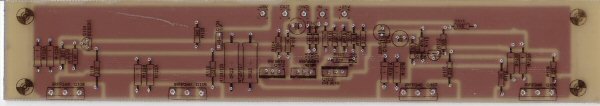
The pic below is from the files area of the Yahoo group I linked to earlier, the folder is labelled:
"Toner transfer pcbs with 8mil width, 8mil clearance specs"and also has a how to pdf
Homebrew PCBs
Regards
James
[SIZE=-1]Hope no one at yahoo minds me borrowing the pic?[/SIZE]
"Toner transfer pcbs with 8mil width, 8mil clearance specs"and also has a how to pdf
Homebrew PCBs
Regards
James
[SIZE=-1]Hope no one at yahoo minds me borrowing the pic?[/SIZE]
Attachments
soundNERD said:o can i get rid of the toner except on the pads, spray it with the protector stuff, then remove the toner on the pads so everything is protected except the pads?
Sounds like they way a PCB shop would do it! No, I just spray the whole board with with that acrylic stuff, which solders through easily. It's basically invisible, being more of a sealer than a paint. If I leave the photoresist on I just solder through it too, but it bubbles a bit around the pads. I imagine toner would work the same.
For a really clean job you could wash the built up board and spray that with something. There are also tin plating solutions availiable, or you can manually tin the tracks with solder and attempt to scrape it off with cardboard or solder wick, but that takes a long time. This is similar to hot air levelling that most PCB shops use. If you're really keen you could try toner transfer onto a screen, screenprint soldermask onto the board, then tin the pads.
The best I ever did was to use spray photoresist to simulate solder mask (a few years ago now). I'll attach a picture if I can work out how.
Attachments
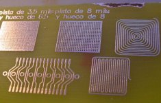
This is a small pcb with 0.4mm lines. Made with photo process and the film printed by imagesetter.
--------------------------------------------
adx, as I see, we do same method for pcb planning!
How do you plan the ”upper” side of pcb with ”negative” soldering-points? Because I using CorelDraw, but I think some program (protel for example) would be much better but I don’t know how protel do it.
An externally hosted image should be here but it was not working when we last tested it.
--------------------------------------------
adx, as I see, we do same method for pcb planning!
An externally hosted image should be here but it was not working when we last tested it.
How do you plan the ”upper” side of pcb with ”negative” soldering-points? Because I using CorelDraw, but I think some program (protel for example) would be much better but I don’t know how protel do it.
Aha, I used Protel to pour a polygon around the pads, then set all the unconnected top pad sizes to zero (any Windows version should work I can't remember if Autotrax does though). It can't "negate" copper though - although you can do this using an image processing program to combine bitmap print outputs. That's actually how I got the "soldermask" inverted.StratoFan said:How do you plan the ”upper” side of pcb with ”negative” soldering-points? Because I using CorelDraw, but I think some program (protel for example) would be much better but I don’t know how protel do it.
I did the no top pad thing to allow more copper on the top layer like your board - those unused pads waste a lot of space! Also on audio designs I don't like the idea of pieces of pad which might intermittently short to component legs, and to some extent making capacitors out of glass epoxy dielectric is to be avoided. I wish I could afford to make plated though boads for DIY stuff though.
I do a lot of contract board designs (it's the only way I actually make money), usually 2 or 4 layer - but the client pays for prototypes! They're not scared to drop a few thousand bucks for a 3 day turnaround 4 layer prototype. Wish they could do the same for the design! (but that's getting better - engineers used to get not much more than minimum wage in NZ).
Oh, I forgot to say that the example of the toner transfer board looks pretty good. With a 1200dpi laser I guess the foot is on the other boot (or whatever). I've heard wax paper works. With 1200dpi you can get reasonably reliable 5 thou (mils for Americans) track / spacing and thus do things some board manufacturers can't. What I'd like to see is someone try making a direct inkjet resist printer out of an old inkjet (it's probably been done, I dare not look).
I always drill with carbide drills - it stops the feathering of the holes, and stops unconnected pads spinning off. Worn carbide is still sharper than HSS after the 2nd hole. You absolutely can not hand wield with carbide bits though: The only thing they like to do more than drill - is break.
I always drill with carbide drills - it stops the feathering of the holes, and stops unconnected pads spinning off. Worn carbide is still sharper than HSS after the 2nd hole. You absolutely can not hand wield with carbide bits though: The only thing they like to do more than drill - is break.
Wax paper? Don't even think about it. The wax will melt and will coat many parts inside your printer with wax. That is not a good thing. I think that perhaps "parchment paper" would work. This is the stuff that chocolate and candy makers use, because stuff doesn't stick to it. You can also bake on it, so it is quite heatproof. Put wax paper in the oven, and you'll get a lot of smoke! Don't expect anything better inside the printer.
I wouldn't recommend wax paper either - I think I was thinking of baking paper (neither would I recommend that!), which may be the same thing. Obviously this is something that you try at your own risk, in an old printer or something, and I can't recommend acting on any ideas you may have to do a full colour silkscreen overlay... Anway the wax should only melt in the fuser - the heated non-stick roller at the output of the printer. The other problem could be wax coming off on feed rollers making them non stick also, not fun.macboy said:Wax paper? Don't even think about it. The wax will melt and will coat many parts inside your printer with wax.
I dont recommend Baking paper
The results were not worth the effort as it smudged due to presure from Ironing.
I had the same problem with sheet sticker backing just oozed under Ironing pressure.
I have had good results the bagasse (suger cane fibre) paper, but you might have trouble finding something equivalent
I think the paper needs a high calcium content or has a Silica Gel coating that dissolves in water?
regards
James
An externally hosted image should be here but it was not working when we last tested it.
, its to thin for the laser printers I've tried, until i double sided taped it to some copy paper.
The results were not worth the effort as it smudged due to presure from Ironing.
I had the same problem with sheet sticker backing just oozed under Ironing pressure.
I have had good results the bagasse (suger cane fibre) paper, but you might have trouble finding something equivalent
I think the paper needs a high calcium content or has a Silica Gel coating that dissolves in water?
regards
James
OK, I found a way that works pretty well with the kinkos paper i have.
heat the board for 2 minutes with it sitting on something hard (I use wood). An ironing board doesn't work.
place the paper where it will go, and it will stick to it.
iron for three minutes with pressure.
put in boiling water for 30 seconds.
peel off as much paper as possible
sand the rest off with VERY fine sandpaper.
etch
works so far. Some of the toner smeared, but i think that was because i printed at 1200x1200dpi, so there was too much ink on the paper. i have to try something like 300x300dpi or 600x600 dpi. but it was simply fixed with an exacto knife.
oops, forgot to say, its etching now, ill post some pics when it is done.
-Mike
- Status
- This old topic is closed. If you want to reopen this topic, contact a moderator using the "Report Post" button.
- Home
- Amplifiers
- Chip Amps
- Making My Own PCBs