I can't view anything on DIYINHK's site as it needs a captcha which is blocked by the Great Firewall.
So you are using an I2S isolator to isolate DSD? My guess is this will introduce rather a lot of jitter. The output impedance of the isolator will depend on the particular chip used - do you know the part number?
So you are using an I2S isolator to isolate DSD? My guess is this will introduce rather a lot of jitter. The output impedance of the isolator will depend on the particular chip used - do you know the part number?
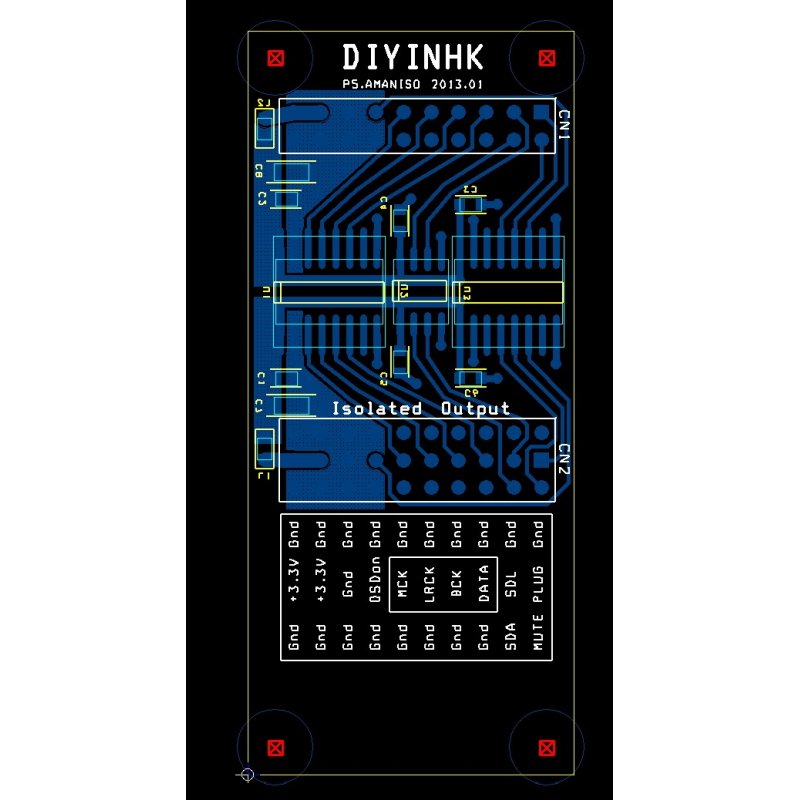
I estimate the output resistance of the isolators at 50ohm (0.2V drop at 4mA output current) assuming they're powered from 5V. At 3.3V the Zout is higher.
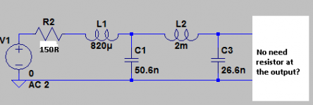
So for 5V supply you'll need a 150R resistor between the ISO7640FM and the LC filter.
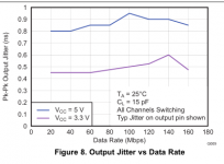
In regard to jitter, the plot shows about 0.8nS which corresponds to modulation of the 50/50 duty cycle at zero (1.4MHz squarewave) by around 0.1%. So you'll be getting about -60dB peak noise due to this jitter. That's not to say your audio bandwidth SNR will only be 60dB though as the bulk of this additional noise will be ultrasonics.
So for 5V supply you'll need a 150R resistor between the ISO7640FM and the LC filter.
In regard to jitter, the plot shows about 0.8nS which corresponds to modulation of the 50/50 duty cycle at zero (1.4MHz squarewave) by around 0.1%. So you'll be getting about -60dB peak noise due to this jitter. That's not to say your audio bandwidth SNR will only be 60dB though as the bulk of this additional noise will be ultrasonics.
Attachments
Last edited:
I've been considering isolation for a multi-channel FPGA based DSD DAC that I'm designing. The conclusion that I came to is that the isolated outputs need to be retimed to eliminate the jitter due to the isolators (and FPGA).
It makes sense therefore to have the main clock source on the output side of the isolators and to feed the clock back to the FPGA through another isolator. This also provides a 'quieter' environment for the oscillator.
It makes sense therefore to have the main clock source on the output side of the isolators and to feed the clock back to the FPGA through another isolator. This also provides a 'quieter' environment for the oscillator.
Butterworth or Chebyshev would be fine - I suggest Butterworth as its simpler to design. The corner frequency depends on you - perhaps 50kHz -3dB would be fine as a first attempt.
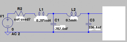
A 4th order LC would have two series inductors and two shunt capacitors, followed by a resistive termination
<edit> Attached a schematic based on a design I did for an ESS DAC. Its Butterworth but 30kHz -3dB.
Now I don't use I2S isolator because introduces a lot of noise.
How can mod the filter for 50 ohms characteristic impedance to drive directly the Amanero?
Using an online calculator result is attached schematic.
Attachments
Last edited:
If you connect this filter to a 100k input impedance (=100k load) then that's totally OK. No need to match the filter to the input impedance.
I think I made the filter with an online calcuator then tidied it up in LTSpice. Can't be sure which online calculator, could have been this one : Chebyshev Pi LC Low Pass Filter Calculator
I think I made the filter with an online calcuator then tidied it up in LTSpice. Can't be sure which online calculator, could have been this one : Chebyshev Pi LC Low Pass Filter Calculator

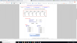

I did mention I wasn't sure it was that calculator ....
Yes sorry. I only want to contrast your design to be sure is good.
- Status
- This old topic is closed. If you want to reopen this topic, contact a moderator using the "Report Post" button.
- Home
- Source & Line
- Digital Line Level
- low pass filter for DSD