Hi all -- Last summer my grandson, a college freshman, heard me talking about my quest for low distortion sine wave oscillators, and asked me why sine waves are a big deal. So I put together a simple tutorial for him here:
Pure beauty: The Sine Wave
This will be familiar to most of you, but you too may have someone who may be interested....
Pure beauty: The Sine Wave
This will be familiar to most of you, but you too may have someone who may be interested....
While I was looking around for the buffer, I was wonder what they use in a HP 3325A function gen (03325-66514, A14 output amplifier assy), as it is spec'd for flatness,level, freq. response testing of the HP 11715A and a HP 8901A that I own. I have no idea of the THD performance of that particular design, but I was intrigued by it none the less, will try to sim that design and see how it performs.
Generally speaking, anything that is optimized for MHz bandwidth is (very) poor for audio frequency distortion performance (and often also noise). A brief look at the schematic suggested that it is a one-stage (folded cascode) opamp; without special techniques, this gives roughly -60 dB to -100 dB THD at full output. If you get around simulating it I'd be interested in your results.
I have checked the datasheet of the OP1-BP and the parameters are excellent. Wish I was able to measure such low distortions as Samuel. I finish at -130 dB even with notch filter.
The datasheet measurements are done with the usual trick of operating the opamp at higher noise gain, then subtracting the noise gain for an input-referred figure. With the ~90 MHz GBW product you can operate it at 60 dB noise gain, so a -130 dB residual drops to -190 dB. The noise rises though, and this ultimately sets a practical limit.
Would you email schematic/parts so I could build one. Or better yet buy one or two all ready made from you? BTW -- How is your osc coming along?
This is a commercial design so of course I can't release most details about the construction. Also you probably don't want to hand-solder a few dozend fine-pitch transistors... But of course you can buy finished amplifiers.
It's not spec'ed for distortion below 600 ohms but it beats developing one my own. There's other things I'd rather be doing and spending on the cost of developing.
What's the cost on these Samuel?
If you forward me the specific operating conditions (output voltage into output load) you're interested in I might be able to do a few specific measurements.
For pricing please contact us through Contact | Weiss Engineering Ltd..
BTW, the pinout is the API 2520 standard, which is still quite common in pro audio for discrete amplifiers and, as far as I know, originates back to the old days of Philbrick.
Samuel
Last edited:
It's not spec'ed for distortion below 600 ohms but it beats developing one my own.
I've just checked the datasheet again--page 11 to 13 show distortion into 200 Ohm.
Samuel
I'm pretty sure Rupert Neve came up with the 2 opamp complimentary
class A bias scheme.
T
I've just checked the datasheet again--page 11 to 13 show distortion into 200 Ohm.
Samuel
I must have been missing some pages. I think I only had two pages.
Been away on a company trip to a distant city. Six hours there and back for a two hour meeting. All expense pain can't complain.
I try again for the data sheet.
I'm pretty sure Rupert Neve came up with the 2 opamp complimentary
class A bias scheme.
T
Sure. But JCX brought it to my attention.
As per Scott Wurcer's suggestion -- Would it be possible to use your OP-BP2? Would you email schematic/parts so I could build one. Or better yet buy one or two all ready made from you?? It seems to be the SOTA and the oscillator of David's could use it to drive low Z loads. I could try it in the front end of analyzer.
BTW -- How is your osc coming along?
THx-RNMarsh
The schematic of the OP1 BP is in the manual.
Generally speaking, anything that is optimized for MHz bandwidth is (very) poor for audio frequency distortion performance (and often also noise). A brief look at the schematic suggested that it is a one-stage (folded cascode) opamp; without special techniques, this gives roughly -60 dB to -100 dB THD at full output. If you get around simulating it I'd be interested in your results.
The datasheet measurements are done with the usual trick of operating the opamp at higher noise gain, then subtracting the noise gain for an input-referred figure. With the ~90 MHz GBW product you can operate it at 60 dB noise gain, so a -130 dB residual drops to -190 dB. The noise rises though, and this ultimately sets a practical limit.
This is a commercial design so of course I can't release most details about the construction. Also you probably don't want to hand-solder a few dozend fine-pitch transistors... But of course you can buy finished amplifiers.
If you forward me the specific operating conditions (output voltage into output load) you're interested in I might be able to do a few specific measurements.
For pricing please contact us through Contact | Weiss Engineering Ltd..
BTW, the pinout is the API 2520 standard, which is still quite common in pro audio for discrete amplifiers and, as far as I know, originates back to the old days of Philbrick.
Samuel
Great.
Samuel can you test it at 84 ohms. This is the lowest load condition it would see from a 50 ohm Z attenuator at -10dB. The load will increase with higher attenuation to a maximum of about 5K. 2.5Vrms input with gains from 0 to 3.2. Can you also test a pair configured for balanced differential into same load. Feedback R values will naturally increase the load so you may include this as well.
Cheers,
That's the "simplified" schematic....
Well it's a product so I doubt such a schematic will be available.
Besides would you really want to deal with smt parts that require a an X10 microscope?
Samuel can you test it at 84 Ohms. This is the lowest load condition it would see from a 50 Ohm Z attenuator at -10 dB. The load will increase with higher attenuation to a maximum of about 5K. 2.5 Vrms input with gains from 0 to 3.2.
From your description it is not clear to me what voltage it should drive into 84 Ohm--2.5 Vrms or 3.2*2.5 Vrms? The latter would not be feasible as it is beyond the output current capability.
Samuel
From your description it is not clear to me what voltage it should drive into 84 Ohm--2.5 Vrms or 3.2*2.5 Vrms? The latter would not be feasible as it is beyond the output current capability.
Samuel
Sorry.
The oscillator output is 2.5Vrms. This is the input driving voltage. The operating gains of the op amp(s) will be between 0 and 3.2. For an output of 2.5Vrms to 8Vrms. With a differential output configuration the total output to load will be between 5Vrms to 16Vrms.
The oscillator output is 2.5 Vrms. This is the input driving voltage. The operating gains of the op amp(s) will be between 0 and 3.2. For an output of 2.5 Vrms to 8 Vrms. With a differential output configuration the total output to load will be between 5 Vrms to 16 Vrms.
8 Vrms into 84 Ohm is too much; you could use two parallel configurations (each with individual feedback network) and sum the two outputs via 100 Ohm resistors (which gives the nominal 50 Ohm output resistance). For such a configuration the 200 Ohm load measurements in the datasheet should be reasonably indicative of the distortion performance. Don't forget to add the noise gain (~10 dB for your case as far as I understand).
Samuel
BTW -- How is your osc coming along?
I'm still working on the PCB layout; here's what I have already:
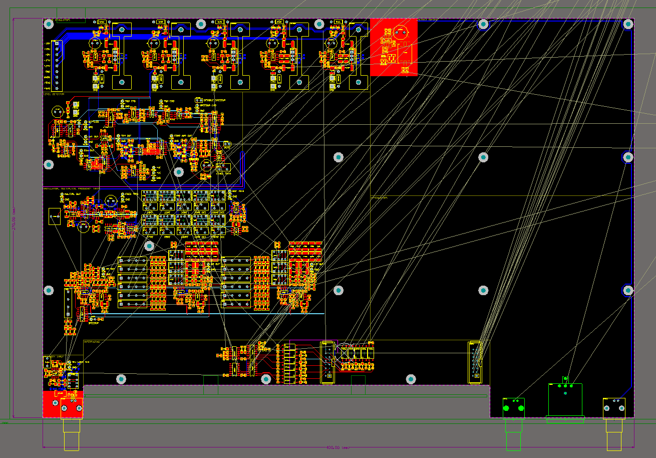
At the top you see the voltage regulators for the five main rails. To the right of the regulators there's the sync output isolation amplifier (transformer-based). Below the three leftmost regulators there's the level detector (S & H stages etc.) and speedup circuitry. Below that, to the left, is the multiplier. To the right, a bank of relays and trimmers for the frequency trims. Below that, the SV oscillator with the relays-, resistor- and capacitor banks for frequency switching. At the bottom of the PCB, in the center, part of the opto-isolators which interface to the frontpanel print. In the bottom-left corner, the injection locking input. In the bottom-right corner, the main and sync output connectors.
Samuel
Samuel -- did you prototype it first or only SIM before doing the PCB layout? That is, do you have measured data, yet?
As noted earlier I have made several design/hardware iterations where the key components (SV filter, multiplier, level detector etc.) were on individual boards. This is the first (and hopefully last) PCB with everything on one board.
Of course I have used simulation extensively, but more to understand and verify the basic operation and functionality of individual sections rather than to estimate the actual distortion. Once the easy things are removed, only secondary distortion mechanisms remain which are either not at all, not accurately or only with unreasonable effort simulated with available low-cost software tools. Examples for these mechanisms are distortion from monolithic opamps, ripple in S & H stages from settling time and dielectric absorption, nonlinear feedthrough in multipliers from transistor mismatch and layout effects.
As I have noted before, I have focused on measuring individual distortion contributors in isolation rather than overall generator performance. Calculations from these isolated measurements, and results from initial overall measurements with the prototype oscillators, indicate that the design beats even the latest AP (particularly WRT THD+N). But this can't be verified before I have the final board in my hands.
Samuel
I still can't get a bottom line on my SVO how are you going to measure this one?
I still can't get a bottom line on my SVO--how are you going to measure this one?
The best bet remain passive notch filters for THD, and analyzer noise RMS subtraction for THD+N.
Samuel
- Home
- Design & Build
- Equipment & Tools
- Low-distortion Audio-range Oscillator