This may not be a major problem if you don't have big currents near this GND pin. If you can show me how the pcb layout is done, I can give you and opinon.Segran said:Sorry Nick, Per-Anders is right! I read the Pin Descriptions in the Datasheet which says just "Device Ground" and have jumped to a false conclusion. I stand corrected....
I wish somebody had pointed out that mistake in my own PCB layouts I have posted here.I will have to re-do the layouts - again....
I can't read them.nickarsow said:Dear P-A,
The PCB layout is two steps above - post#40 in a .ZIP file.
Regards
Nick
I wonder what proportion of interested readers can see what you have designed?
SpittinLLama said:Nick, can you elaborate more on why you consider the National PCB awful? I'd really like to know specifics that you dislike about it. Just not right for your design?
Thanks,
-TH
Reminds me of a line rendered by Dan Ackroyd to Jane Curtin on SNL back in 1978...
Jack
As explained, gerber is a special file format, not a common one but luckily there are free gerber viewers out there. Personally I prefer Viewmate.nickarsow said:Dear Andrew,
These files are gerber files made on PROTEL DXP.
As they are gerber files - anyone could read them. ( I hope so ).
http://pentalogix.com/Products/ViewMate/register.cfm
Your JPG's is ten times bigger than they have to be. Try to reduce quality next time.nickarsow said:The bottom overlay is too big either in JPG - I'll try other way.

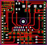
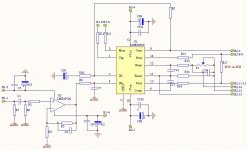
... but where are the connections for the wires? H2, 2-3 is ground in the pcb but in the schematic it's something elsenickarsow said:Analogue GND is shown by GND bar and marked as AGND , while power ground is marked as earth.

- Status
- This old topic is closed. If you want to reopen this topic, contact a moderator using the "Report Post" button.
- Home
- Amplifiers
- Chip Amps
- Lme49830