1100mA less what passes through the emitter resistor. That is not a miss type.
Look at the formula.
6.9 mA into the base and a gain (hFE) of 160 gives a collector current of ~ 1100mA
But, try to find a device that has a gain for 160 when passing that collector current.
You are likely to find a few devices that can output ~580 to 600mA for a base current of 6.9mA, i.e. a gain of 85 @ Ic=590mA.
Last edited:
ahh, but there is more...
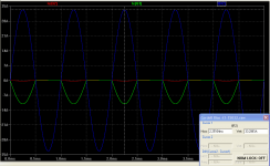
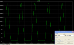
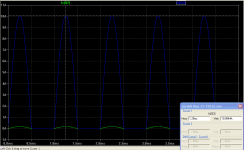
The clipping behavior looked like the voltage limit from earlier simulations. So, I upped the voltage again, this time to 60v. New plot, no clipping. Driver is still working - taking the 6.9ma and making 158ma and the 32.8A overall.
So, is spice the wrong tool for this? Will this driver run out of gas?
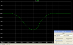
I bumped the voltage to 100v and set the load at .25 ohm, and guess what the driver started clipping. The waveform is different than the voltage limited type clipping. The final plot is of the driver waveform. Obviously, the SOA has also been exceeded for the driver and the outputs, but, what I believe these simulations say is that the LME49811 output of 6.9ma can drive an darlington configuration into 4 ohms and beyond, with the appropriate driver transistor. But, the configuration is supply voltage limited. Next test will look at the configuration with a predriver to see if it changes the voltage limitation issue.
Comments, critique.
The clipping behavior looked like the voltage limit from earlier simulations. So, I upped the voltage again, this time to 60v. New plot, no clipping. Driver is still working - taking the 6.9ma and making 158ma and the 32.8A overall.
So, is spice the wrong tool for this? Will this driver run out of gas?
I bumped the voltage to 100v and set the load at .25 ohm, and guess what the driver started clipping. The waveform is different than the voltage limited type clipping. The final plot is of the driver waveform. Obviously, the SOA has also been exceeded for the driver and the outputs, but, what I believe these simulations say is that the LME49811 output of 6.9ma can drive an darlington configuration into 4 ohms and beyond, with the appropriate driver transistor. But, the configuration is supply voltage limited. Next test will look at the configuration with a predriver to see if it changes the voltage limitation issue.
Comments, critique.
Attachments
this implies an output stage with a gain of ~200. You must be asking the simulator the wrong questions.Driver is still working - taking the 6.9ma and making 158ma and the 32.8A overall.
So, is spice the wrong tool for this?
Hi,
try a load of 1r3 driven to 28Vac. i.e. Imax~30Apk.
This will show what the simulator thinks are the currents in the various stages.
This is roughly the amplifier current capability I would design for a maximum power of 200W into a 4ohm speaker.
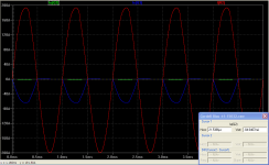
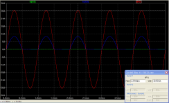
When I run it as specified, I get 21.5Apk. I(R2) is the current through the 1R3 load resistor.
Second plot is where I put the probe for the driver transistor current.
Third plot is the current for the driver transistor(Q2).
Fourth plot is the current for one of the output transistors (Q3).
I just thought maybe I need to convert your 28Vac into RMS. - it works, 30Apk. Plots in the next post.
Attachments
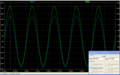
28Vac 8 1.414 = 39.59v for simulator input voltage.
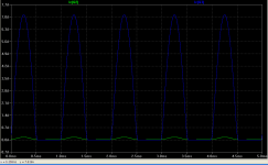
pk Load at driver 193.389mA. (Q2)
pk load at one output transistor 10.0544A(Q3)
pk Load at driver 193.389mA. (Q2)
pk load at one output transistor 10.0544A(Q3)
Attachments
3pair output stage each passing 10Apk.
Output from the driver 193mApk.
Base current to each output device ~64mA.
This implies a gain in the output devices of ~150.
Either the model is wrong or you have asked the wrong question.
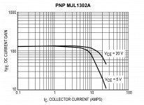
The gain of a typical mjl3281 @ 10A is ~65 @25degC.
A reasonable minimum to design with is probably around 35 to 40.
ONsemi specify 45@8A and 12@15A.
Output from the driver 193mApk.
Base current to each output device ~64mA.
This implies a gain in the output devices of ~150.
Either the model is wrong or you have asked the wrong question.
The gain of a typical mjl3281 @ 10A is ~65 @25degC.
A reasonable minimum to design with is probably around 35 to 40.
ONsemi specify 45@8A and 12@15A.
3pair output stage each passing 10Apk.
Output from the driver 193mApk.
Base current to each output device ~64mA.
This implies a gain in the output devices of ~150.
Either the model is wrong or you have asked the wrong question.
The gain of a typical mjl3281 @ 10A is ~65 @25degC.
A reasonable minimum to design with is probably around 35 to 40.
ONsemi specify 45@8A and 12@15A.
Hi Andrew,
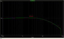
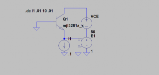
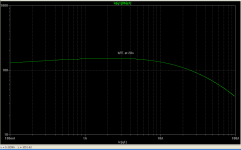
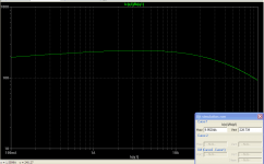
Seemed like a lot of gain to me as well. Question is does hFe rise with voltage? The spec sheet does imply a bit of this, look at the hFe at 20v vs 5v. It's clearly higher at 10amps at 20v than at 5v. But, does it rise to the level of 150 at 50v at 10A? I'm using Andy_C's model and went to his simulation for the transistor alone. The following are the schematic used for the test and the output from the test at 5v, 20v and 50v. I varied VCE using the 5v, 20v and 50v. When I made the screen capture it was set at 50v. The plots show the hFe at 10A at 50v to be 228. It's well beyond my pay grade to know if the model is accurate at this voltage. Someone will have to ask Andy_C. But, the result, for what it's worth, is consistent between the model simulation and the amp simulation.
Ken
Attachments
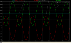
look at your simulation and read off the Vce when driving 30A through 1r3.
Hi Andrew,
Are these what you're looking for?
Ken
Attachments
Hi,
can I assume that for this resistive load that when V@emitter peaks that coincides with Imax to the load (1r3)?
Then look at Vce when Ipk=10A/output device.
I think you will see ~8Vce. Check this value by hand calculation to show that you have asked the correct question.
Things change when the load is reactive. I don't have the brainpower to work that out for you. But I can say that Vce will certainly be much higher @ Ipk when the load is a complex C+L+R, since we know that voltage and current are not in phase.
Hi,
can I assume that for this resistive load that when V@emitter peaks that coincides with Imax to the load (1r3)?
Then look at Vce when Ipk=10A/output device.
I think you will see ~8Vce. Check this value by hand calculation to show that you have asked the correct question.
Things change when the load is reactive. I don't have the brainpower to work that out for you. But I can say that Vce will certainly be much higher @ Ipk when the load is a complex C+L+R, since we know that voltage and current are not in phase.
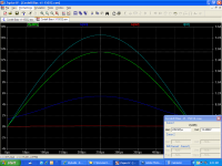
Hi Andrew,
To your first question, yes.
If I shoot for a Ipk of 10A/3output devices or about 3.333A Ipk, I get Vce of about 13.44v.
(this is with a 13.2v sine input and 4r load) should I use the same 1r3 load with a different input voltage?
Ken
Attachments
I posed this question in the Solid State forum Spice Simulation thread. Response from Bob Cordell.
Originally Posted by klewis
Hi,
I have a question for you guys. Working on a simulation for the output end of an amp, running with 50v rails, I found the output transistors reaching high hfe at this voltage. (I was driving a 1r3 load) I was using Andy_c's mjl3281 models for the outputs. To back check these results, I ran the simulation from Andy_c's website with VCE set to 50v. At this setting the transistors showed hfe of about 228 at 10A.
Is this a believable number? Does hfe rise with voltage?
Thanks
Ken
Hi Ken,
The short answer is yes, hfe rises with voltage for a BJT. This is the Early effect. The higher reverse voltage across the base-collector junction increases the size of the depletion region, encroaching on the base and making it thinner. Thinner base usually increases hfe.
For your specific case, the number you are seeing for hfe seems high, especially at that current where you would expect some beta droop.
Some models have odd sensitivities to certain variables under certain conditions. Check with Andy_c on this. He can probably shed some light on it.
I don't have that model in front of me, but the first thing I would look at is the value of BF. BF is usually higher than peak beta of a transistor. However, if it is more than a factor of two higher than peak beta, I have sometimes discovered that the model has some undue sensitivities.
Cheers,
Bob
Andrew,
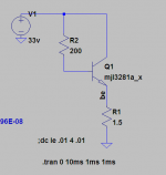
I got around to measuring the current output into different loads for a mjl3281. With a setup as shown in the schematic, 33v rail.
For a 8 ohm load 46ma of current at the tranistor base, 2.767A output.
For a 3 ohm load, 47ma of current at the base, 5.304A output. hFe =112
For a 1.5ohm load, 62ma of current at the base, 7.220A output. hFe = 116 For the simulation at 1.5ohm load, it predicts 10.344A.
Using my limited understanding of things, to get the 30Apk through the outputs, 30A / 116 = 258ma needs to be produced by the driver from the approx. 7ma drive current. That's an hFe for the driver of 36. seems very do able.
What do you think?
Ken
Attachments
this does not match the data given by the manufacturers.For a 3 ohm load, 47ma of current at the base, 5.304A output. hFe =112
For a 1.5ohm load, 62ma of current at the base, 7.220A output. hFe = 116 For the simulation at 1.5ohm load, it predicts 10.344A.
Dear All,
I have an question regarding this pre-driver current thing.
Rod elliot says on his site:
"For the sake of simplicity, if bipolar output transistors have a gain of 20 at the maximum current into the load, the drivers must be able to supply enough base current to allow this. If the maximum current is 4A, then the drivers must be able to supply 200mA of base current to the output devices.
Prior Stages
The stages that come before the drivers must also be able to supply sufficient current for the load imposed. The Class-A driver of a bipolar or MOSFET amp must be able to supply enough current to satisfy the base current needs of bipolar drivers, or the gate capacitance of MOSFETs.
Again, using the bipolar example from above, the maximum base current for the output transistors was 200mA. If the drivers have a minimum specified gain of 50, then their base current will be ...
200 / 50 = 4mA"
My question is. Let's take this 4A in where we need 200mA. What if we use 4 pairs of output transistors with 4A each. (means our total output current goal is 16A) Do we need then 1000mA drive current for al transistors? or still the same 200mA?
With kind regards,
Bas
Dear All,
I have an question regarding this pre-driver current thing.
Rod elliot says on his site:
"For the sake of simplicity, if bipolar output transistors have a gain of 20 at the maximum current into the load, the drivers must be able to supply enough base current to allow this. If the maximum current is 4A, then the drivers must be able to supply 200mA of base current to the output devices.
Prior Stages
The stages that come before the drivers must also be able to supply sufficient current for the load imposed. The Class-A driver of a bipolar or MOSFET amp must be able to supply enough current to satisfy the base current needs of bipolar drivers, or the gate capacitance of MOSFETs.
Again, using the bipolar example from above, the maximum base current for the output transistors was 200mA. If the drivers have a minimum specified gain of 50, then their base current will be ...
200 / 50 = 4mA"
My question is. Let's take this 4A in where we need 200mA. What if we use 4 pairs of output transistors with 4A each. (means our total output current goal is 16A) Do we need then 1000mA drive current for al transistors? or still the same 200mA?
With kind regards,
Bas
Bas,
It seems that you're confusing the current production capacity of the transistor with it's gain. Do you want to make 16A of current? If so, then divide the 16A by the hFe.
So, 16A / 50hFe = 320ma of drive must be provided by the driver transistor.
If the driver has the same 50hFe, then it needs 320ma / 50 = 6.4ma of current.
Using Rod's example of an 20hFe for the output transistor (which is a pretty low hFe) the math would be 16A / 20 hFe = 800ma.
If the driver has a 50 hFe, this it needs 800ma / 50 hFe = 16ma of current.
The reason for using 4 pairs of output transistors is to keep these transistors within their SOA. Their SOA is found by looking at the SOA for the voltage you are using and the current at that voltage. I don't know what voltage you're planning on using, but, know that as the voltage goes up the SOA current falls off rapidly for BJTs. It's important to look closely at the data sheets.
Hope this helps.
Ken
Dear Ken,
Thanks a lot for the explanation. It did help a lot!
If you don't mind, to see if I really get it correct, one more question.
I want to avoid a 3 stage EF setup. Listening test turned out that I liked the sound of paralleled Darlingtons more. I suspect this is because you can avoid the higher capacitance associated with bigger driver transistors needed to feed all the transistors.
Therfore I decide for a new design with a individual driver for each transistor.
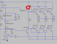
Please take a look at my schematics: http://img35.imageshack.us/img35/5425/thermaltrak22.gif
Ignore the driver transistor ID in my schematic. Instead I want to use the super spec Toshiba 2SC6072/2SA2190 drivers: http://www.semicon.toshiba.co.jp/docs/datasheet/en/Transistor/2SC6072_en_datasheet_091221.pdf
To see if my calculations are correct please follow me.
The NJL3281D indicates in the SOA curve 7A (1sec) by 27 VDC.
So 7A each transistor is my reference. I use 3 NJL3281D's means 21APK. However, since each transistor has it;s own individual driver, I only need to worry about the 7A
The hFE for the NJL3281D by 7A is 170 worst case.
7/170=0,041A
So each 2SC6072 driver must deliver 0,041A, since one driver feeds one transistor.
Now since I use 3 drivers in parallel the total current delivered by 3 drivers is 3*0,041=0,124A. Am I still going correct here...?
The hFE for the 2SC6072 is an amazing 200 by 0,2A (25 degrees celsius)
Means the LME49811 must be able to deliver 0,124/200=0,00061A. If this is truth this system must have a low distortion, a tremendous current capacity and the LME chip has an easy life.
Am I doing correct here? Please any comment about this design are welcome as well I tried it in another topic but not so much response

Thank you in advance.
With kind regards,
Bas
Last edited:
Bas the first link doesn't work, can you make a .png image of it and attach to the post?Dear Ken,
Thanks a lot for the explanation. It did help a lot!
If you don't mind, to see if I really get it correct, one more question.
I want to avoid a 3 stage EF setup. Listening test turned out that I liked the sound of paralleled Darlingtons more. I suspect this is because you can avoid the higher capacitance associated with bigger driver transistors needed to feed all the transistors.
Therfore I decide for a new design with a individual driver for each transistor.
Please take a look at my schematics: http://img35.imageshack.us/img35/5425/thermaltrak22.gif
Ignore the driver transistor ID in my schematic. Instead I want to use the super spec Toshiba 2SC6072/2SA2190 drivers: http://www.semicon.toshiba.co.jp/docs/datasheet/en/Transistor/2SC6072_en_datasheet_091221.pdf
To see if my calculations are correct please follow me.
The NJL3281D indicates in the SOA curve 7A (1sec) by 27 VDC.
So 7A each transistor is my reference. I use 3 NJL3281D's means 21APK.
The hFE for the NJL3281D by 7A is 170 worst case.
21/170=0,124A
So each 2SC6072 drive must deliver 0,124A.
Now since I use 3 drivers in parallel the total current delivered by 3 drivers is 3*0,124=0,371A. Am I still going correct here...?
The hFE for the 2SC6072 is an amazing 200 by 0,2A
Means the LME49811 must be able to deliver 0,371/200=0,0018A
Am I doing correct here? Please any comment about this design are welcome as well I tried it in another topic but not so much response
Thank you in advance.
With kind regards,
Bas
I see an hFe at 7A for the NJL3281 of about 85 not 175. So, 21A/85 = 247ma
I don't know why you would use 3 drivers... you only need one driver for these three output tranistors. You'll want to put 10 ohm resistor on the base leg of each output transistor to help balance the current load between each one - they won't have exactly the same hFe. The driver math would be 247ma/200hFe = 1.2ma drive current from the LME49811 (which make about 6ma).
Regarding the 2SC6072, I've had trouble with these very fast tranistor driving the Thermal Traks. I'm not exactly sure why, but, I was trying to use the Toshiba with 100mhz speed and it didn't want to run. I would suggest that you put in MJE15032/33's to make sure it runs then try swapping in the 2SC6072s. The hFe is not as high, but, you've got current to spare.
Ken
Bas the first link doesn't work, can you make a .png image of it and attach to the post?
I see an hFe at 7A for the NJL3281 of about 85 not 175. So, 21A/85 = 247ma
I don't know why you would use 3 drivers... you only need one driver for these three output tranistors. You'll want to put 10 ohm resistor on the base leg of each output transistor to help balance the current load between each one - they won't have exactly the same hFe. The driver math would be 247ma/200hFe = 1.2ma drive current from the LME49811 (which make about 6ma).
Regarding the 2SC6072, I've had trouble with these very fast tranistor driving the Thermal Traks. I'm not exactly sure why, but, I was trying to use the Toshiba with 100mhz speed and it didn't want to run. I would suggest that you put in MJE15032/33's to make sure it runs then try swapping in the 2SC6072s. The hFe is not as high, but, you've got current to spare.
Ken
Dear Ken,
Here the schematic attached.
I got you about the NLJ3281D. You took the worst case scenario with -25 degrees celsius which indeed gives an hFE of about 85.
One reason to go with multiple drivers is to give the system more current headroom, but most important, the distortion of the LME49811 rise excessive above 1,2mA remember measurements from Panson.
With kind regards,
Bas
Attachments
- Status
- This old topic is closed. If you want to reopen this topic, contact a moderator using the "Report Post" button.
- Home
- Amplifiers
- Chip Amps
- LME49810/STD03 parallel pairs