Russ White said:
No it is not current limited. At least according to the design engineer I called to ask.
How about a current-limited voltage regulator for the chip?
panson_hk said:
How about a current-limited voltage regulator for the chip?
That is a very interesting idea....
Russ White said:I suppose the only way to know for certain would be to short the output with an ammeter.
Or to be slightly nicer, hook up the Fig. 3 test circuit in the datasheet with +/-50V rails and load the output with a 470 Ohm 5W resistor. Drive the amp with say a 1Khz sine wave and gradually turn up the wick until the output starts to clip on a CRO. The maximum output current capability is then simply Vpeak/R. Hopefully the chip won't expire.
The slew rate limit can also be measured by increasing the frequency until the output is a triangle wave, then measure the slope in V per microsecond. Ccomp influences the slew rate.
I just haven't had time to try this with my samples....
yes a CCS set to quiescent +20% and then shunt regulate that extra 20% to ground.panson_hk said:How about a current-limited voltage regulator for the chip?
The chip is then protected at quiescent current level until the shunt starts to reduce it's demand to try to keep the supply voltage up, plus peak/transient demand from any supply caps after the CCS.
Simple and short circuit proof.
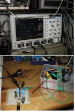
The Cc in the prototype is 22 pF. I then measured some curves using AP S1. The output residual noise is about 45 uVrms (BW = 22 kHz). Several THD vs output level curves are shown in the pdf file (note the input impedance of S1 is 100 kHz). My next step is to load the circuit similar to that of headphone amp.
Attachments
Hi,
what connections have you got to ground (0V)?
The output should be open circuit for checking output offset.
Will this chip operate correctly with both outputs unconnected?
If you know the ground currents then you can calculate the difference between Icc & Iee.
If there is zero ground current, then Icc=Iee.
AndrewT said:Hi,
what connections have you got to ground (0V)?
The output should be open circuit for checking output offset.
Will this chip operate correctly with both outputs unconnected?
If you know the ground currents then you can calculate the difference between Icc & Iee.
If there is zero ground current, then Icc=Iee.
Input (IN+) is grounded via Rin. Am I answer your question?
Yes, offset was measured with output open circuit. The ground current is 4 mA, exactly the difference between Icc and Iee. Is it normal?
Hi,
you are getting 4mA flowing into the ground connection from Vcc.
Why do National show 2mA flowing out of the ground to Vee?
Your input pin ground current <1uA and is swamped by others.
Why is your circuit flowing in the opposite direction?
Is your 4mA the mute current?
you are getting 4mA flowing into the ground connection from Vcc.
Why do National show 2mA flowing out of the ground to Vee?
Your input pin ground current <1uA and is swamped by others.
Why is your circuit flowing in the opposite direction?
Is your 4mA the mute current?

AndrewT said:Hi,
you are getting 4mA flowing into the ground connection from Vcc.
Why do National show 2mA flowing out of the ground to Vee?
Your input pin ground current <1uA and is swamped by others.
Why is your circuit flowing in the opposite direction?
Is your 4mA the mute current?
The mute current measured is 100 uA.
panson_hk said:Quiescent current Icc = 12 mA and Iee = 8 mA were measured. Does anyone have these data? Are they supposed to be not identical? Data sheet says Icc=11 vs Iee=13 mA. Output DC is 0.4 mV with input grounded.
Should I ignore what you type in future?panson_hk said:I didn't not measure the exact Icc and Iee, but +I and -I. Now is okay!
What are you on?
AndrewT said:
Should I ignore what you type in future?
What are you on?
Sorry Andrew. I should not do typing while measuring.
glennb said:
Or to be slightly nicer, hook up the Fig. 3 test circuit in the datasheet with +/-50V rails and load the output with a 470 Ohm 5W resistor. Drive the amp with say a 1Khz sine wave and gradually turn up the wick until the output starts to clip on a CRO. The maximum output current capability is then simply Vpeak/R. Hopefully the chip won't expire.
The slew rate limit can also be measured by increasing the frequency until the output is a triangle wave, then measure the slope in V per microsecond. Ccomp influences the slew rate.
I just haven't had time to try this with my samples....
Why use 470 Ohm?
I think the test I recently did is similar to what you described. I tried different resistor at the output of Fig 3 with 1 kHz sine wave and +/- 60 V rails. With 600 Ohm load, the chip clips at about Vpeak = 28V. The current at this point is 47 mA. However, the chip clips at a much lower output for 100 Ohm.
Attachments
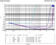
Hi Panson,
starting from the left, I think you are showing us loadings of
100r, 600r, 1k0, 10k & open superimposed.
There is a big jump from 100r to 600r and again another big jump from 600r to 1k0.
It appears that the chip is much happier with the 1k0 load.
This would indicate a current gain of 300 is required to drive 8ohm speakers and about 600 to drive 4ohm speakers.
Neither of these gains are available from single BJT devices so it looks like a driver and output EF stage must follow the chip.
Alternatively a FET output stage could be implimented.
AndrewT said:yes a CCS set to quiescent +20% and then shunt regulate that extra 20% to ground.
The chip is then protected at quiescent current level until the shunt starts to reduce it's demand to try to keep the supply voltage up, plus peak/transient demand from any supply caps after the CCS.
Simple and short circuit proof.
Hi Andrew,
Thanks for you comment on output drive capability!
For current-limited regulator, you proposed a shunt regulator? The chip's Iq is 11/13 mA. If the CCS is set at 50 mA, a shunt transistor will consume about 39 mA x 60 V = 2.34 W in idle mode. Will it be too much? How about a series regulator with current limit?
Panson
- Status
- This old topic is closed. If you want to reopen this topic, contact a moderator using the "Report Post" button.
- Home
- Amplifiers
- Chip Amps
- LME49810 - a new cousin for LM4702