@tomchr
I don't know what is wrong with you and what is a reason for such cynical writing?!
How anyone can have a DATA if they do not conduct an test with some method and one very trusty method I explained.
I only can guess that your writing is with intention to kick me off from the forum (and you did it) and probably strongly related to your Modulus-86 which for some reason have some idea VERY SIMILAR to BatoMM design which is done 2-3 years before yours!?
Intrigued I had a look at this BatoMM. It is a composite Amp, but there the similarities end. So really not sure what you are getting so upset about. Composite amplifiers are decades old (maybe older than you are) so its not as if you have invented anything new. The remote sensing on a chipamp you have is AFAIK new.
Yeh, some people whom do not go by the book messes up the thought those who live by it. Going by the book is not a bad start. The ancient Chinese had ceased to innovate when they started to rely on only following the books. Sometimes some ideas may look crazy, but we just have to accept that some people tend to do things differently. Personally I like to understand the process more than just looking at data. Test methods tell you more if you really understand what is basically going on.
I'm completely OK with innovation. But once you start making claims based on faith rather than science and start claiming that the laws of physics are "just a theory" is where I get off.
I think it's rather concerning that those of us who point out that physics work in a certain way get thrown out as "not thinking outside the box". We all have to abide by the laws of physics, whether we think inside or outside the box.
~Tom
Last edited:
The remote sensing on a chipamp you have is AFAIK new.
Yeah, but done all the time on power supplies - and has been since, oh, about the beginning of time. An audio power amp is eerily similar to a power supply with a modulation input...
")
~Tom
I don't know what is wrong with you and what is a reason for such cynical writing?!
Oh, there are many things wrong with me. Where would you like me to start...

How anyone can have a DATA if they do not conduct an test with some method and one very trusty method I explained.
You claimed to have developed a new clamping method for a chip amp and performed an experiment to show how well it worked. All I asked for was the data from your experiment. How much of an improvement in thermal performance did you measure?
~Tom
Oh, there are many things wrong with me. Where would you like me to start...
You claimed to have developed a new clamping method for a chip amp and performed an experiment to show how well it worked. All I asked for was the data from your experiment. How much of an improvement in thermal performance did you measure?
~Tom
why you dont belive man he has no reason for lie on stupid forum. and he actualy tried his experiment in real life what you didnt do.
if you so fired up by data then go build that device as suggested by him and do your measurments. and be thankful for him sharing his idea with you.
one question , how to measure chips die temperature ?
The measurement of the die temperature of a smart power chip is very complex. The issue is the area of the output semiconductors as a percentage of the overall die, as well as the methodology for measurement of the junction temperature.
Typically, one of the junctions on the active device is used as the metric. For example, a bipolar transistor emitter-base junction in forward bias at constant current is a good metric. The device is forced to dissipate a known power for a high duty cycle, and when turned off, measure the E-B junction voltage within 100 uSec of turn off.
The two copper blocks are ok, but the block on the topside of the package has about 40 to 60 mils of loaded epoxy to transfer the heat through. Epoxy of this type has a thermal transfer coefficient about two orders of magnitude below that of copper.
The bonding wires are either supported within the potting compound directly, or there is a flexible glob top encapsulation of the wires to prevent thermal cycling failure of the wires. If there is a glob top coating, it is optimized for thermal expansion and flexure properties, NOT thermal transfer.
Honestly, if one wanted the very best with a package of this type, take the bottom finish down to a mirror finish using first 1500 grit, then 4000 grit on an optically flat surface. Then, use that new graphene sheet stuff as an interface to a really flat copper surface. Once the spread envelope has become very large, bog standard insulation grease and insulating shims can be used without much penalty.
ps..if you want more info, you'll have to ask Jan Didden for it....next month.
PPS. isolated backside?? chuck it, you need to get down to the copper tab the chip is metallurgically bonded to.
jn
Last edited:
why you dont belive man he has no reason for lie on stupid forum.
The man said: I have a gizmo that will provide great improvement of the thermals of a chip amp.
I asked: Would you please show how much improvement can be had with your gizmo?
The man took his toy and went home. That's unfortunate...
At no point did I say that I though he was lying. Nor did I even suspect him of lying. I don't know where you get that from. I do happen to know physics well enough to be able to determine whether his claims are valid. I don't believe they are. I don't believe his clamp provides any significant advantage over a piece of bar stock clamped across the package. "The Man" claimed there was an advantage, and all I did was to ask him to quantify the advantage. I really don't see anything wrong with that.
and he actualy tried his experiment in real life what you didnt do.
if you so fired up by data then go build that device as suggested by him and do your measurments. and be thankful for him sharing his idea with you.
Why? If he's performed the experiment already, why doesn't he just share the data? Isn't that the purpose of a forum thread?
one question , how to measure chips die temperature ?
You can get an estimate by measuring a diode junction voltage on die. This will only give you the temperature locally where the diode is, which may be different from other points on the die.
~Tom
PPS. isolated backside?? chuck it, you need to get down to the copper tab the chip is metallurgically bonded to.
Yep. For the best thermal conductivity, use a package with a metal back.
~Tom
I'm guessing the TF version has a metal tab inside which is then enclosed in mold compound.
If you want a chipamp with a metal back, I suggest using the T version. If you don't want to mess with thermal pads, get the TF version. Both can support the full output power given the right size heat sink, so unless you're really trying to push the thermals, there's no advantage of the T version, honestly.
~Tom
..............................
~Tom
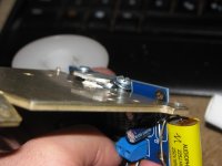
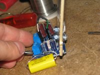
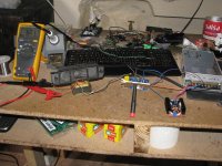
well i dont know maths well but this worked over 20 minutes and didnt seem to get more hot ,at least to my measurments by hand , while chips back side was hotter then aluminium piece , aluminium part actualy got pretty warm,almost hot.
powered by +-12v from mean well supply and buck boost converter for dual rail. it was outputing 8v AC into 2.1 ohms trafo secondary and on trafo primary was speaker. 50 hz sine generated by audacity...
you know maths i hope you can pull some valid data out of this but i think front chip side actualy does transfer heat well! better than expected!
Attachments
...
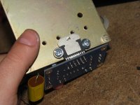
Distributing the clamping pressure evenly across the IC is a good idea. All you need for that is a bar across the IC package that you clamp to the heat sink. You don't have to use fancy materials or fancy shaped clamps for this.
...
From the o r i g i n a l "multi3886" amp:

and

Rowland +3 parallel and -3 parallel (+/- 3 para/bridge)
[if i recall, they're inverted and the pot is to adjust the -in 'res' to gnd (on the neginput, to balance the + and - input impedance on the 3886; to get min out offset or min input dist. ... )
...errr, and fancy transformer inputs ... ]

from
Jeff Rowland LM3886 Amplifiers
you don't even wanna know the date ...
... this is ol' schooool!
( ͡° ͜ʖ ͡°)
Last edited:
I was just talking with a manufacturer about heat dissipation of aluminum and copper, they mentioned that copper conducts heat better but aluminum dissipates heat better, is there any truth to that?The measurement of the die temperature of a smart power chip is very complex. The issue is the area of the output semiconductors as a percentage of the overall die, as well as the methodology for measurement of the junction temperature.
Typically, one of the junctions on the active device is used as the metric. For example, a bipolar transistor emitter-base junction in forward bias at constant current is a good metric. The device is forced to dissipate a known power for a high duty cycle, and when turned off, measure the E-B junction voltage within 100 uSec of turn off.
The two copper blocks are ok, but the block on the topside of the package has about 40 to 60 mils of loaded epoxy to transfer the heat through. Epoxy of this type has a thermal transfer coefficient about two orders of magnitude below that of copper.
The bonding wires are either supported within the potting compound directly, or there is a flexible glob top encapsulation of the wires to prevent thermal cycling failure of the wires. If there is a glob top coating, it is optimized for thermal expansion and flexure properties, NOT thermal transfer.
Honestly, if one wanted the very best with a package of this type, take the bottom finish down to a mirror finish using first 1500 grit, then 4000 grit on an optically flat surface. Then, use that new graphene sheet stuff as an interface to a really flat copper surface. Once the spread envelope has become very large, bog standard insulation grease and insulating shims can be used without much penalty.
ps..if you want more info, you'll have to ask Jan Didden for it....next month.
PPS. isolated backside?? chuck it, you need to get down to the copper tab the chip is metallurgically bonded to.
jn
A friend does some process that allows building traces right on aluminum, seems like it was developed to help dissipate heat for LED application. Wondering what more potential application that could be applied to. Also wondered about thermal cycling as well.
It is much easier to just take your pick on any single point that is wrong, proves a point more clearly...Oh, there are many things wrong with me. Where would you like me to start...
You claimed to have developed a new clamping method for a chip amp and performed an experiment to show how well it worked. All I asked for was the data from your experiment. How much of an improvement in thermal performance did you measure?
~Tom
Though I am curious how one could clamp the LM3886 to let heat dissipate better.
Without knowing the output current you can't say much about your test.
Try connecting a resistor to the output.
?
if transformer conected on output resistance is 2.1 ohms and across that 2.1 ohms i have 8v AC at 50hz .
isnt that 30w output of lm?
and isnt that 3.5 amps?
i connected 8ohms speaker on primary, secondary to lm outputNO.
How did you measure the resistance? With a DMM at DC?
Now you are testing with 50Hz with a speaker connected to the secondary.
trafo is 230v primary > 24v secondary ac , 25VA at 50hz rated, it started smelling bad after 10 minutes of this torture, so i assumed that it had more than 25 w at output of lm3886 but assumptions are always bad so i would like to test this your way but i am not sure how exactly.
primary dc resistance is 200 ohms secondary 2ohms ,wire thickness is primary: 0,5mm , secondary i cant measure . thats all i have
- Status
- This old topic is closed. If you want to reopen this topic, contact a moderator using the "Report Post" button.
- Home
- Amplifiers
- Chip Amps
- LM3886 Thermal Experiment (with data)