But will they sound fine?.... only building to listen and compare to a reference and test it using non biased evaluators.
Looks great..no doubts....but there's a lot of things that looks great but are not great.... sometimes sound ordinary as Hugh told.... well..he can say things about as he built.
regards,
Carlos
Only I should add that the 'unbiased evaluators' doesn't exists. Listening is always a 'biased process' that depends on many subjective and cultural background factors. Some will love sounds that are awful for others. And also it cannot be determined by vote what a 'good' sound is, maybe you can determine a 'popular sound', what the majority likes, and maybe that sound is not for me, so it is strictly personal.
Cheers
Arturo
Kenpeter :
OLG (voltage) is not increased by a source follower. Go figure...
And unfortunately neither is this specific example giving us any
current gain...
I agree about slew, thats why the driver stage is better here:
His output stage abusing same JFET at exactly same current.
Yet pulling SE against fixed CCS, is only half as capable as the
push-pull circuit that is driving it. Defeats its own purpose...
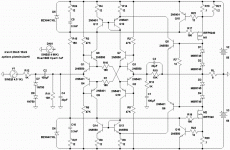
OH NO, the more loaded is the VAS the lower voltage swing will be (OLG), that's why the need of a buffer, expose the VAS to a light load and let the buffer do the brute force against the OPS. The output impedance of the buffer is determined by the EF (U1) not the CCS, you can replace the CCS by a resistor of 10K, 5K, 1K and the output impedance of the buffer will be almost the same, the only difference will be the quiescent current of the buffer, even more you can eliminate the CCS and the circuit will continue working. And yes there is a current gain with the buffer as it raises the output impedance of the VAS ... and so on backwards.
Cheers
Arturo
Kenpeter :
Output impedance is overwhelmingly set by the closed loop, not by local impedance.
Source vs drain follower topology does not dictate how low the final number can be.
Available current swing runs out of steam twice as fast with the SF+CCS output.
Yes an No, it is all about the amount of output distortion tolerable, among other factors. The more loaded VAS the more output distortion.
That's the controversy of direct VAS driving, EF2, or EF3 (depending on OPS devices), nevertheless you will need a minimum current gain (for a given load), regardless the FB loop, that is Ai>=Av(constant)*(Zi/Zo). So if you set the maximum distortion allowable, the minimum damping factor and the minimum input impedance for a fixed Av through the BW, it is very likely that a buffer stage will help the amp. performance. It is up to each concrete implementation.
Cheers
Arturo
I am still i doubt, will it work with real not so perfect matched J-fets...how to keep the center from floating...??..
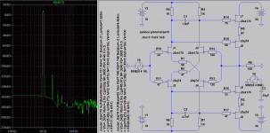
Only thing I can think to randomize it more would be another JFET .model
I do have three or four slightly different .models for these same JFETs.
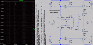
Offset maybe, but distortion don't look all that sensitive to mismatch...
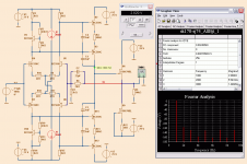
Attachments
And I might add something non-intuitive about closed loops.
All impedances inside a closed loop system are LOW.
Yeah, anywhere in the middle of the loop too.
Was so proud I had designed a Triode + PNP Concertina
phase splitter that was all DC coupled, had +/- 1/2Mu
voltage gains and absolutely equal output impedances.
Open loop, it made a huge improvement in symmetry.
But closed loop Williamson, it was no better or different
than plain phase splitter with unequal local impedances.
The loop drove both impedances to be absolutely equal.
Kenpeter :
Arturo, if you had an EF3 OPS. Why add another EF buffer to make EF4?
Are we forgetting the OPS is already a buffer? How many stages can we
tolerate to be in a loop before layout starts to affect stability?
The fewer EF's the better for stability, despite stability is a primordial concern there are other issues to take account, I understand that EFn includes de OPS as the last buffer, but it is not important to stick in a semantic issue. Including a buffer stage between VAS and OPS or not, is a trade off, what are average and peak current demands?, it's a 10W OPS or 16 device 2KW OPS?, the distortion?, stability?, BW? offset? ... etc. infinite solutions ... I am not advocating the use of more or less buffers a priori, it depends on the minimum that satisfy the rules of design, that are completely arbitrary because are 'my/your rules', if you achieve same or better results that full fills the 'rules' with no intermediate buffers, no doubt, that's a better design.
Cheers
Arturo
actually the impedances inside the loop can be quite high, even in a closed loop. the impedance of a VAS is still quite high (unless the feedback is sampled at the VAS, then the impedance would be low). between the VAS and output (where the feedback is sampled from) you have buffer amps, and the load impedance seen by the high impedance VAS is the output impedance times the output device betas (including any pre-drver and driver stages. let's say we have a VAS with a 20k output impedance and it's in an amp with a closed loop. the output impedance of the amp is 0.01 ohms. there are 3 EF stages between the VAS and output terminal. the beta of the predriver transistors is 200, the driver beta is 100 and the output devices 50. the impedance "reflected" to the VAS is 200x100x50x0.01 or 10k. the action of feedback would make the amp do whatever is required to maintain equilibrium at the inputs, so the VAS would be driven harder to make up the difference. this in effect seems to lower the impedance of the VAS, until the VAS reaches it's physical limitations, and the loading of the VAS begins to have side effects.
The problem is this: PP AB output stages have highly variable input impedance owing to device switching transitions.
With lots of global fb, the VAS papers over these cracks, but wherever correction is strong there is inevitably more distortion.
As Arturo says, a buffer on the VAS will soften the worst effects of these wild impedance changes.
Technically, there is no argument that a buffer on the VAS is a GOOD thing.
But you have to build and listen to it. Sometimes you find that what is better technically sounds bad. And I've noticed that what sounds bad to one guy, often sounds bad to another. Over a sample of ten listeners, you can often reach consensus.
I favor Class A SE buffers for the VAS since the distortions introduced are mostly even order.
Hugh
Current source, sink, and bandwidth are all important.
Impedance in the middle of a closed loop is irrelevant.
No matter what might happen open, its forced low.
My point was that the "buffer" presented here could
only source+sink half as much current swing as VAS.
Sure, loaded VAS might now run into trouble. But that
lame buffer would have run to the same trouble twice
as early.
Hi
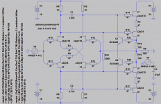
if you do the output stage with lateral mosfets you can skip the VBE multiplier and create the bias with a simple resistor as biasspreader network...
You could fix the spread across Lineup's R20+R21 bias resistors by returning
current to his VAS stage. In my oddball example you also see a 15K on the
flipside of the VAS to balance against those same bias correcting currents.
Yeah, theres a whole lot more strange going on here. But the bias is all
I really wanted to show. The rest may not be relevant to this thread.
Anyways, takes hot output devices completely out of the bias equation.
Lineup's output introduces two hot emitter drops of uncertainty after the
bias spreader. Probably not a big deal, I'm just making conversation...
At 5.6mA (.12W), nothing about Lineup's circuit is going to get especially
hot anyway...
As you beef up that output, or add EFs, it might become relevant...
For purpose of this thread, ignore my Class B Schottkys and pretend they
are Lineup's Class A resistors.
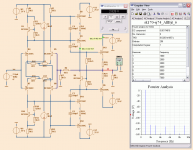
Attachments
Last edited:
This bias scheme doesn't make a whole lot of sense at such low current.
I would not normally have needed 100R resistors. I'm just showing how
you can use cold transistors to regulate bias, and not let a hot output
device make that decision.
---oops---
Drew Q2 PNP upside down, strange the sim still worked fine that way...
I thought VBE was supposed to avalanche like a Zenier around 5V???
Attachments
Last edited:
- Status
- This old topic is closed. If you want to reopen this topic, contact a moderator using the "Report Post" button.
- Home
- Amplifiers
- Solid State
- LINEUP Input-VAS, idea