See also post #12.
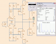
ALL JFET circuit again.
THD 0.000 052 %
This is close to a perfect amp with gain=1
And can be optimized for other gains, too.
All harmonics below -130dB!!
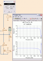
The AC Analysis shows curves freq & phase
With such an amp you DO NOT start 'improving'.
Do you?
It will only make things more or less worse.
ALL JFET circuit again.
THD 0.000 052 %
This is close to a perfect amp with gain=1
And can be optimized for other gains, too.
All harmonics below -130dB!!
The AC Analysis shows curves freq & phase
With such an amp you DO NOT start 'improving'.
Do you?
It will only make things more or less worse.
Attachments
The test SPICE does not show anything strange in circuits I published.
On the contrary it shows very good figures regarding distortion.
I can not answer for modified circuits published by other
No, no. Nothing strange in yours. Excepting an output stage capable
of delivering only half the current of the VAS that drives it. But I do
understand the reasons. So long as whatever comes after don't ask
for more than +/-3mA drive, its not a problem...
I am the one that posts the strange drawings. About to eliminate
40ohm degeneration between FETs and rely upon current feedback
as previously shown to hold a steady bias. Those 40R resistors only
serve to linearize local current gain at the expense of open loop
voltage gain and closed loop voltage linearity. I think I can make
em' disappear, or at least shrink a smaller value to our advantage.
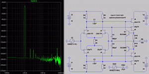
-140 on all harmonics. Go figure...
Next: Is there any reason those 1K's couldn't be increased, and run everything off the 24V supplies?
Yep. Try 1K2 @ 24V! Doesn't hurt a thing, still under -140...
Next: Is there any reason those 1K's couldn't be increased, and run everything off the 24V supplies?
Yep. Try 1K2 @ 24V! Doesn't hurt a thing, still under -140...
Attachments
Last edited:
Hi,
have a look at Patent US3,908,170 of Buhler/Philco-Ford Corp. from 1975.
The patent describes a HV-hybdrid video amp. It shows a single ended implementation of the complementary-VAS-cascode.
I found it quite interesting, but couldn´t get it to run well in simulation.
jauu
Calvin
have a look at Patent US3,908,170 of Buhler/Philco-Ford Corp. from 1975.
The patent describes a HV-hybdrid video amp. It shows a single ended implementation of the complementary-VAS-cascode.
I found it quite interesting, but couldn´t get it to run well in simulation.
jauu
Calvin
Despite the very good numbers showed by lineup and kenpeter, I have a question: Is this amp (lineup) intended for headphones? if it is, the OPS showed with be short of 'punch' I guess (was kenpeter arguments), another issue not addressed is the thermal stability of DC OFFSET (very critical for headphones) in real implementation kenpeter's schema will be better as it has Q1 and Q2 compensation of the bias point, a solution is an output capacitor to couple the load, with the drawbacks known. I would like to see a more 'real' amp schema with different (and nasty) loads, the real gain(s), DC OFFSET at different temperatures ... etc.
BTW there are several schemas that achieve ppm's THD's similar to showed, and I will not introduce more noise posting some of mine ... I am much more interested on the REST of important issues I pointed above.
Cheers
Arturo
BTW there are several schemas that achieve ppm's THD's similar to showed, and I will not introduce more noise posting some of mine ... I am much more interested on the REST of important issues I pointed above.
Cheers
Arturo
Kenpeter:
DC offset will depend how well matched are the four input JFETs.
The next step might be cascoding drains all to the same voltage.
Yes, but in reality that so close matching is difficult to achieve over a range of temperatures, with a complementary input upper and lower legs with different temp. profiles you can't get such matching perfection and thermal balance so some drift is expected, the VAS will amplify the drift and the NBF will reduce it but not with a perfect precision cancellation within a range of 30° or 40° temperature, unless you do AC coupling for the FB loop which is your case, but not lineup amp which is DC coupled. A 10mV to 30mV offset doesn't harm power speakers, but headphones are very sensible to >10mV offsets.
Cheers
Arturo
Last edited:
Hi Lineup!
Please comment:
Hi Lineup!
As far as I can see, you wont get double gain by using complement pairs. Look at it this way: One transistor will need a certain drive to pass a certain current. The other transistor will need an equal amount of drive just to pass the same current. ( which it will have to , since they are in series. ) So you will get the same gain as with only one transistor ( your example one ).
You might get some linearization of the FETs though.
Thorsten Larsen
Last edited:
True, drive voltage double is canceled when transconductance is halved.
I still think this plan is superior for PSRR. Differentially driven with most
power noise cancelled in the common mode. In the VAS itself, a high Z
drain or collector points at rail noise, rather than low Z source or emitter.
I don't see how the JFET is linearised? (current or voltage linearity?)
Expending gain to linearize current would be working directly against
the objective of a linear voltage amplifier. Only care transconductance,
and the direct coupled local loop makes voltage linearity.
Take away all feedback that "linearizes" the FET in the current domain,
and the voltage domain distortion of the loop goes down -10db.
Try to have it both ways at once, you get a tube amp that might sound
nice, but isn't necessarily linear in either domain.
Last edited:
Kenpeter :
My FB is AC coupled??? When did that happen?
You mean #37?
Yes #37, C1 (100uF) that's AC coupling, R13 connected to 0V directly is DC coupling, not the case shown in #37
Cheers
Arturo
Last edited:
Anyway, with or without the biasing trick, if direct coupled (as it is lineup's circuit) it will have much more thermal drift than AC coupled FB loop, maybe you will need a DC servo ... new problems, among others is the clipping asymmetry at low freq. <100HZ, and the stored charge at the integrator = slow response.
I am still not seeing where this thermally drifted DC offset happens?
The input compares to the output, and matched parts thermally bonded have the same drift...
Again, N's don't have to match or drift with the P's. But the input side does have to match
and drift with the feedback side. Why is this circuit causing you to worry so much more on
drift than another with the same matched and bonded component pairs at the input?
Last edited:
Things in reality are much more complex, the theory takes account on what 'should' happen given a hypothetical math. perfect model and other unrealistic assumptions (the ideal OP amp, infinite input impedance, zero output impedance, infinite OLG) , physical real devices departs slightly but enough from theory, to make arise all this effects, that's why nowadays chip makers uses some built-in mechanism to address this issue. I have experienced at simm's and in practice (there are some topologies more or less prone to drift, other discussion). Do some temp. (30°-100°) simm's and you'll verify that in a DC FB loop this drift could be as high +/-100mV or more. Maybe a +/- 30mV drift is OK for a power amp, but not for a headphone amp, that's my point.
Cheers
Arturo
Cheers
Arturo
Last edited:
- Status
- This old topic is closed. If you want to reopen this topic, contact a moderator using the "Report Post" button.
- Home
- Amplifiers
- Solid State
- LINEUP Input-VAS, idea