Andy_c just one another remark:
" First, why does the Leach amp need 4 temperature compensation diodes when it's only compensating 2 junctions (the output stage NPN and PNP)?"
And the drivers too (MJE15030/31). The dissipation of this transistors increase with the higher output current, so it's important to compensate them too.
Another thing:
The temperature of the junction in the output devices allways higher than the temperature of the sensors, so You need more diodes.
Sajti
peranders said:
Check very carefully! You have in fact 6 transistors!
Wich 6? As I wrote, I count only 4
Sajti
I counted all emitter follower transistors but I'll guess only four of them can be hot.sajti said:Wich 6? As I wrote, I count only 4
So you have at least 4 PN-junctions which need to be taken care of.
sajti said:Remove one sensor diode from the circuit is not a good solution.
Here's a quote from Dr. Leach's web site concerning this. The only reason he's using four diodes instead of three is for mechanical reasons of orientation of the leads coming in and out of the heat sink. He needed an even number.
From the Leach web site
The original amp used 2 diodes. I changed to 3 to after measuring the bias current as a function of heat sink temperature and found the amp to be thermally undercompensated. But with 3 diodes, the two leads from the diodes to the circuit board come out on opposite sides of the heat sink. I added a 4th to recitfy this problem and found that the amp didn't seem to be thermally overcompensated.
sajti said:And the drivers too (MJE15030/31). The dissipation of this transistors increase with the higher output current, so it's important to compensate them too.
The book by Self has a graph of driver dissipation vs. the voltage delivered to the load (figure 12.1 in his book). As the caption of this figure says "In all variations of the EF configuration, power dissipation varies little with output".
The situation with complementary feedback output pairs is quite different though. For this type of output stage, the driver dissipation has a 2:1 variation with the output voltages that Self considered.
However, I could envision a case where the EF dissipation would vary a lot more. If many output transistors were used in parallel, then the output current requirements of the driver would be much greater, and the power dissipation in the drivers would vary a lot more. But in the case of the Leach amp, there are only two output transistors in parallel.
If You remove one diode, You have to redesign the resistor values to get same bias. BUt of course it's possible.
The driver dissipation depending some other things too:
1, Is the driver mounting on same heatsink as the output devices?
2, Is the driver in same case as the output devices? (darlington)
The input current of the output devices can be much higher. Mr Leach set the bias of the drivers to 6mA. But when the output current goes up to 10A (it's common with 4ohm speaker), the driver will gives some 200mA current (MJLs have B about 50@5A). This current is 30times more!
In my experience is that the MJE15030/31 works better with higher bias, so I use them with 80mA.
Sajti
sajti said:
The input current of the output devices can be much higher. Mr Leach set the bias of the drivers to 6mA. But when the output current goes up to 10A (it's common with 4ohm speaker), the driver will gives some 200mA current (MJLs have B about 50@5A). This current is 30times more!
Okay, let's put some numbers to this case! If we take the average power for a half-wave rectified current and sinusoidal voltage (subtracted from Vcc) over a half cycle, we get:
P = Vcc*Ipk*2/pi - Vpk*Ipk/2
for the power dissipation.
Vcc = 56
Ipk = 0.2 for driver, 5 for output
Vpk = 40
Driver: P = 3.13 W
Heat sink theta_ca = 23.2 (Aavid data sheet)
Transistor theta_jc = 2.5 (OnSemi data sheet)
Driver temperature rise = 3.13 * (2.5 + 23.2) = 80.4 deg C
Output: P = 78.25 W
assume theta_cs = 0.1 deg C/W (thermal washer)
theta_jc = 0.7 from OnSemi data sheet
theta_cs = 47/50 deg C/W from Wakefield 423K data sheet
Output transistor temperature rise = 78.25*(0.1+0.7+47/50) = 136.2 deg C
Note: constant 56 V supply is probably not a very accurate assumption!
So the Vbe delta with this application of power is 136.2/80.4 = 1.7 times as great for the output stage as the driver because of the larger junction temperature change. So if "one Vbe" is one output stage Vbe, the number of Vbe's to compensate is 2 + 2/1.7 = 3.2 for this case of 200 W into 4 Ohms.
Interesting...
andy_c said:
Okay, let's put some numbers to this case! If we take the average power for a half-wave rectified current and sinusoidal voltage (subtracted from Vcc) over a half cycle, we get:
Andy, I agree with your calculation with one exception: the ops devices aren't conducting (other than the bias) in the other half of the cycle. so power dissipation will be 50% of your calculation.
you do run the risk of thermal damage, however, if you size the heatsink using the 50% factor if you play loud bass for an extended period of time.
Hmmmm....
in this case we have no ouput transistors any more! If the ambient temperature is 25degree, and we increase the junction temperature with 136.2, we killed the MJL (Tjmax=150).
I think the peak dissipation sholud be Pdmax=(Ut^2/Rload)*.2=(56^2/4)*.2=157W
This is for 4 pcs. of output devices.
It's about 40W each.
assume theta_cs = 0.1 deg C/W (thermal washer)
theta_jc = 0.7 from OnSemi data sheet
With this data, the temperature rise 32degree, over the heatsink.
The calculation for drivers is more complicated. If I multiply the load with the B of the outputs (50) the result is 200ohms.
The dissipation in this case is:3.17W for two drivers. About 1.6W each.
In most amplifier the drivers use same heatsinks as the outputs. In my new amplifier I will use separated large heatsinks for the drivers.
Sajti
sajti said:I think the peak dissipation sholud be Pdmax=(Ut^2/Rload)*.2=(56^2/4)*.2=157W
the maximum peak power dissipation takes place when the transistors are outputing 50% of the rail on the load (and the transistors themselves). so power dissipation should be (Ut/2)*(Ut/2/Rload)=196w.
millwood said:
the maximum peak power dissipation takes place when the transistors are outputing 50% of the rail on the load (and the transistors themselves). so power dissipation should be (Ut/2)*(Ut/2/Rload)=196w.
I think I made mistake. The dissipation I want to calculate, not the peak, but the maximum dissipation. This is valid at the 60% of the max. output power.
Sajti
sajti, the 60% number looks awefully close to the theoretical efficiency of a push-pull ops (75% with ideal transistors I think).
However,t he maximum power dissipation on the output devices takes place when 50% of the rail voltage is drop'd on the load. That is pure math.
Output device dissipation = V * I = V * (Vt-V)/Rload.
That value reaches its maximum when V=Vt/2.
However,t he maximum power dissipation on the output devices takes place when 50% of the rail voltage is drop'd on the load. That is pure math.
Output device dissipation = V * I = V * (Vt-V)/Rload.
That value reaches its maximum when V=Vt/2.
"sajti, the 60% number looks awefully close to the theoretical efficiency of a push-pull ops (75% with ideal transistors I think)"
The 60% percent means that if You have 100W amplifier, it will dissipate the maximum, when the output power is 60W (60% of maximum output power).
"75% with ideal transistors I think)"
78.5% is the maximum with ideal transistors.
Sajti
The 60% percent means that if You have 100W amplifier, it will dissipate the maximum, when the output power is 60W (60% of maximum output power).
"75% with ideal transistors I think)"
78.5% is the maximum with ideal transistors.
Sajti
millwood said:
Andy, I agree with your calculation with one exception: the ops devices aren't conducting (other than the bias) in the other half of the cycle. so power dissipation will be 50% of your calculation.
Ahh, now I see what the error was. I only integrated over a half cycle of the signal, but at the end I divided the results by pi instead of dividing the results by 2*pi. Serves me right for doing this stuff late at night.
") I'll post the corrected results tonight when I get home from work.
I'll post the corrected results tonight when I get home from work.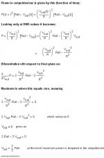
Re: Power in outputdevices
Jens: why is P=I^2*V?
JensRasmussen said:Correct me if I'm wrong
All this talk about maximum power in output transistors confused me, so I tried this:
I that wrong?
No DC current in the devices is taken into the equation
\Jens
Jens: why is P=I^2*V?
Correction to previous post (power and junction temperature calculations)
First, thanks to Millwood for pointing out the factor of two error in the power calculations I posted. This post contains the corrected calculations for the case that sajti brought up;
Corrected power equation:
P = Vcc*Ipk/pi - Vpk*Ipk/4
Also, sajti quoted a transistor B of 50, which is lower than the worst case value of 80 at 25 deg C from the data sheet. So I'll use 80 for B. That's a 25 deg C worst case number, so the actual B will be higher both because the junction temperature will be higher than 25 deg C, and because of statistical variations.
Vcc = 56
Ipk = .125 for driver, 5 for output
Vpk = 40
Driver: P = 978 mW
Heat sink theta_ca = 23.2 (Aavid data sheet)
Transistor theta_jc = 2.5 (OnSemi data sheet)
Driver temperature rise = .978 * (2.5 + 23.2) = 25.1 deg C
Output: P = 39.13 W
assume theta_cs = 0.1 deg C/W (thermal washer)
theta_jc = 0.7 from OnSemi data sheet
theta_cs = 47/50 deg C/W from Wakefield 423K data sheet
Output transistor temperature rise = 39.13*(0.1+0.7+47/50) = 68.1 deg C
This gives a junction temperature of 50.1 deg C for the drivers, and 93.1 deg C for the output stage. Much more reasonable than the wrong results I posted previously. Also note that the rise above ambient for the output stage is 68.1/25.1 = 2.71 times greater than that of the drivers. So the effective number of Vbe's we're compensating for is 2 + 2/2.71 = 2.73. We're at less than 3 now. Given a tight thermal coupling of the sensing diodes to the output transistor, 3 may be the closest number of diodes to use.
First, thanks to Millwood for pointing out the factor of two error in the power calculations I posted. This post contains the corrected calculations for the case that sajti brought up;
Corrected power equation:
P = Vcc*Ipk/pi - Vpk*Ipk/4
Also, sajti quoted a transistor B of 50, which is lower than the worst case value of 80 at 25 deg C from the data sheet. So I'll use 80 for B. That's a 25 deg C worst case number, so the actual B will be higher both because the junction temperature will be higher than 25 deg C, and because of statistical variations.
Vcc = 56
Ipk = .125 for driver, 5 for output
Vpk = 40
Driver: P = 978 mW
Heat sink theta_ca = 23.2 (Aavid data sheet)
Transistor theta_jc = 2.5 (OnSemi data sheet)
Driver temperature rise = .978 * (2.5 + 23.2) = 25.1 deg C
Output: P = 39.13 W
assume theta_cs = 0.1 deg C/W (thermal washer)
theta_jc = 0.7 from OnSemi data sheet
theta_cs = 47/50 deg C/W from Wakefield 423K data sheet
Output transistor temperature rise = 39.13*(0.1+0.7+47/50) = 68.1 deg C
This gives a junction temperature of 50.1 deg C for the drivers, and 93.1 deg C for the output stage. Much more reasonable than the wrong results I posted previously
. Also note that the rise above ambient for the output stage is 68.1/25.1 = 2.71 times greater than that of the drivers. So the effective number of Vbe's we're compensating for is 2 + 2/2.71 = 2.73. We're at less than 3 now. Given a tight thermal coupling of the sensing diodes to the output transistor, 3 may be the closest number of diodes to use.More junction temperature stuff...
Just for grins, we can find the maximum power dissipation for 4 and 8 Ohms and figure out the junction temperature rise for driver and output stage. The power can be written as:
P = Vcc*Vpk/(pi*RL) - Vpk*Vpk/(4*RL)
Differentiating with respect to Vpk and setting the derivative to zero results in:
Vpk = 2*Vcc/pi = .637*Vcc
Plugging that result back into the power equation gives:
Pmax = (Vcc*Vcc)/(pi*pi*RL)
Vpk = 35.65
For 8 Ohms, Pmax = 39.7W, Ipk=4.46A (2 output devices), Ipk=55.7mA (driver)
Fot the output stage worst case into 8 Ohms, the junction temperature rise is:
39.7*(0.1+0.7+47/50)*0.5 = 34.5 deg C
For the driver, the power dissipation is:
56*.0557/pi - 35.65*.0557/4 = 496 mW
Temperature rise = .496*(2.5 + 23.2) = 12.8 deg C (driver)
So for the worst case output stage dissipation into 8 Ohms, the junction temperature rise is 34.5/12.8=2.70 times as high as for the driver. The number of effective Vbe's to compensate is 2 + 2/2.70 = 2.74.
For 4 Ohms, Pmax = 79.4W (for two devices), Ipk=8.91A (2 output devices), Ipk=111mA (driver)
For the output stage worst case into 4 Ohms, the junction temperature rise is:
79.4*(0.1+0.7+47/50)*0.5 = 69.1 deg C
For the driver, the power dissipation is:
56*.111/pi - 35.65*.111/4= 989 mW
So the junction temperature rise is:
.989*(2.5 + 23.2) =25.4 deg C
So the ratio of junction temperature rises is 69.1/25.4=2.72. The effective number of Vbe's to compensate is 2 + 2/2.72=2.74.
Addendum: Well, looking back at the data sheet, I misread the worst case B as 80 when it should be 60. But looking at the typical B curves, 80 seems like a totally reasonable number considering the elevated junction temperatures we're dealing with. There's always something...
Andy,
if You check my numbers about the dissipated power, You will find that my results are same, for the output devices.
I calculate the power devices with 5A each (sorry I did'n specify output power), and the Onsemi datasheet recommend to match the output transistors for B=50@ Uce=5V, and Ic=5A. This is why I used B=50. But Your point of view is acceptable for me too, because I measured 26pcs. of MJL21193/94, and 90% of them gives higher B, than specified.
Well right now we have to compensate 2.74 times 2.2mV/C. (Of course this is true when we use different heatsinks for the drivers) How we can calculate the next step?
If I apply the common single transistor bias circuit, the multiplying rate is 4 because I have to create bias voltage for 4 transistors. It's about 2.4V. But in this case my compensation is 4 times 2.2mV/C, if the junction temperature of the sensor device is same as the output, and driver.
Sajti
- Status
- This old topic is closed. If you want to reopen this topic, contact a moderator using the "Report Post" button.
- Home
- Amplifiers
- Solid State
- Leach amp bias diodes