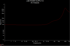
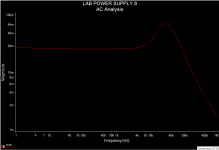
I'd use standard miller compensation around Q5, probably with a resistor in series like you have now to get sensible components values for a nice loop crossover frequency. The current R3 does not do much though. It won't have much effect until about two decades above the loop gain crossover frequency.
Mega, is it painful to be so damn right, so damn often? 😀
I followed your suggestion and I have even better stability. Not only that, ripple on the output is actually less, both with and without a load (unbelievable?!).
I tried 100pF and 2.2k in series, then 3.3k - giving me better stability. Transient response is much faster but shows some damping. I'll play with the values some more to find the best result.
Hmm file is large so I zipped it
A quick explanation
V1 simulates the main transformer's secondary, it is 25V currently but I plan to wind onto it a few extra turns to make it 27V. There is a set of resistors and switches to select the appropriate shunt resistor for the current limiter. it cxan be removed if we do not care about current limiting. The pass transistors are Q1 Q2 Q5. There is a 100uF cap C2 at the output. past the output there is a constant current system to allow me to simulate load conditions (Q6, Q8 etc). It is not part of the circuit.
V2 is a 32VAC source that supplies the "electronics". U1 and D10 provide a very smooth voltage at the base of Q3. What comes out of Q3 should be pretty stable and clean at about 38 VDC.
U2 is the voltage regulator. The real opamp is the MC33072A and not the AD820 but the former does not simulate at all. The voltage regulator is a diff amp, receiving the output voltage at the +in and comparing it to a fixed voltage at the -in provided by a zener, D8 at 30VDC and a pot is used to select 0-30V. The U2 chip can swing very close to the the negative rail which is very important, otherwise it would keep the control transistor Q7 open all the time. Q7 is like Q5 in your circuit.
U3 and U4 is the current limiter. U4 receives a small voltage and amplifies it by 10x and references it to ground. U3 then receives this voltage and compares it with a fixed value (yet another zener, D6) and when it crosses it goes into current limiting by driving Q4. In that case Q4 would be fighting Q7.
This is really it. Points to be solved are the compensation caps on the op-amps, it seems the caps are quite important as well as the negative feedback. I have tried various combos with comparators and so on, this is the best (simulation) solution.
Another point to worry is that if the op-amps go into oscillation then it is only their output pin's internal current limiting that will stop them from burning Q7 or Q4. I have tried a series resistor at the base or a small resistor at the emitter to limit the current flow at error conditions.
Attachments
You may have a devil of a time to stabilize this - it won't run stable for me in simulation. I've swapped out several opamps (known good models) and haven't had any luck.
I think you may want to shift your focus to getting your basic CV section stable on its own, then add the current limiter back in and stabilize that.
Based on what I just went through, I would work on stable operation first, then concentrate on ripple performance.
I think you may want to shift your focus to getting your basic CV section stable on its own, then add the current limiter back in and stabilize that.
Based on what I just went through, I would work on stable operation first, then concentrate on ripple performance.
The supply is stable. I added a 100uF cap to the output and ran the transient response again. It had a small negative impact of the TR but overall, I think it is a good addition. With the cap in place, the output looks less 'noisy' (noisy is REALLY not a term that applies here. I actually connected my headphones to the output through a 1uF cap and had a listen - nothing...no hum, no buzz, nothing at all.)
I have produced a new schematic. It has a couple of additions that may be worthwhile:
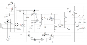
A cap multiplier on the doubler supply. To his credit, akis got me thinking and even though Q8 (previously Q5) can handle it, why burden it with excessive ripple to fight with. Simulation says this gives a marginal improvement in output ripple.
Also, I have added some missing items. Bypass caps on the raw supply and doubler supply, and a couple of caps and diodes around the LM317. Again, these will give a marginal improvement.
Next, it is back to the board layout to implement these changes and squeeze in the digital pot layout. The boards will, once again, get bigger.
I have produced a new schematic. It has a couple of additions that may be worthwhile:

A cap multiplier on the doubler supply. To his credit, akis got me thinking and even though Q8 (previously Q5) can handle it, why burden it with excessive ripple to fight with. Simulation says this gives a marginal improvement in output ripple.
Also, I have added some missing items. Bypass caps on the raw supply and doubler supply, and a couple of caps and diodes around the LM317. Again, these will give a marginal improvement.
Next, it is back to the board layout to implement these changes and squeeze in the digital pot layout. The boards will, once again, get bigger.
You may have a devil of a time to stabilize this - it won't run stable for me in simulation. I've swapped out several opamps (known good models) and haven't had any luck.
I think you may want to shift your focus to getting your basic CV section stable on its own, then add the current limiter back in and stabilize that.
Based on what I just went through, I would work on stable operation first, then concentrate on ripple performance.
It works for me, I use version 11. However it, and most other circuits past some basic complexity, is severely affected by irrelevant things like positioning and probes: you add a probe and it does not work anymore. You move the probe one junction to the left and then it starts to work again... Also mind interactive elements like pots: when you adjust a pot it sometimes goes haywire. You need to stop + start the sim at the new pot setting.
The big Enemy is, "convergence error, timestep too small". I usually fiddle with "interactive simulation settings" and set a minimum time and that fixes the problem 50% of the time. The other 50% is cursing and swearing time.
If you replace the op-amps you have to pick those that can approach the "negative" rail. Which ones did you choose? The AD820 is the one that has worked best for me.
I nicked an idea from a NS datasheet: you can add a FET before R2, it makes ripple coming out of the zener much less. It really works (on the simulation) 🙂
On the NS datasheet "R2" does not exist, but then you have to choose an appropriate FET with very small forward transconductance (or whatever the term is). I added the "R2" to keep the current low flowing through the zener using a FET from my draw. Attached diagram.
On the NS datasheet "R2" does not exist, but then you have to choose an appropriate FET with very small forward transconductance (or whatever the term is). I added the "R2" to keep the current low flowing through the zener using a FET from my draw. Attached diagram.
Attachments
It works for me, I use version 11. However it, and most other circuits past some basic complexity, is severely affected by irrelevant things like positioning and probes: you add a probe and it does not work anymore.
I'm running it on the trial version of 11 and it isn't stable. It is running very slowly as well (a bad sign in my experience) with it taking taking 20-30 seconds to step thru .5 seconds of operation.
After I loaded it, I had to change the 2N5459 to 2SK170 (no MS model for that) and I ran it. It started to oscillate at .443 seconds and then halted at a convergence error. Maybe something was corrupted while zipping it.
This is not an overly complex circuit and that is not typical performance for MS.
Tit for tat, I'll attach mine and you can check out its performance. Give it about 20 seconds (MS timestep clock) for it to settle in. Adjust R18 for 10VDC after the LM317 and R19 for ~1.3VDC at the anode of D9.
View attachment LAB POWER SUPPLY.6.zip
I air-wired the cap multiplier for the doubler supply:
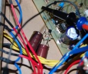
and it works as expected.
The new filtered output of the doubler supply:
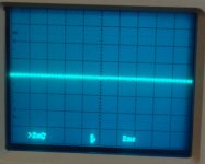
Compare that to the first photo in post #113 and there is an obviously massive reduction in ripple. In terms of ripple reduction at the supplies main output, there isn't a noticable difference. Was it a waste of time? Maybe, but we (here at DIY Audio) excel at that, chasing the ultimate, unmeasurable. 🙂 Anyway, my first cap multi, so it is good experience for me.

and it works as expected.
The new filtered output of the doubler supply:

Compare that to the first photo in post #113 and there is an obviously massive reduction in ripple. In terms of ripple reduction at the supplies main output, there isn't a noticable difference. Was it a waste of time? Maybe, but we (here at DIY Audio) excel at that, chasing the ultimate, unmeasurable. 🙂 Anyway, my first cap multi, so it is good experience for me.
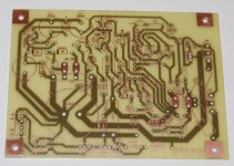
New layout:
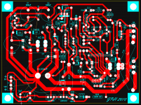
I found a mistake on the schematic, at C7 and fixed it on the board.
This has become quite a complex beast of a board! More detailed than many of the amplifiers seen on this site, even. I have come to appreciate how challenging it is to design and build a good quality power supply and I'll definitely make good use of that knowledge in future projects.
Rather than throw them out,
Hands up out there in TV land if anyone wants the boards that these new ones will replace. Shown in post #41, they will be stripped of the actives and major passives, leaving only the 1/4 watt resistors.
For the cost of postage, they can be yours. 🙂
....PM me if you want them.... please don't post here.
The first boards is dressed and installed for testing:
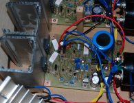
bear with me folks, these next 3 are probably the last scope screen shots I'll show.
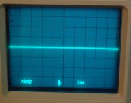
Output at 15VDC:
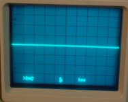
Output 15VDC at 2A:
Transient response:
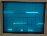
I believe I have it nailed. No oscillation, no output ripple.
Mission accomplished and then some thanks to some VERY excellent advice from Mega and akis. Thanks! 🙂
Next, I need to make the board for the other supply, load it up and get the digital pots hooked up again.

bear with me folks, these next 3 are probably the last scope screen shots I'll show.
Output at 15VDC:

Output 15VDC at 2A:

Transient response:

I believe I have it nailed. No oscillation, no output ripple.
Mission accomplished and then some thanks to some VERY excellent advice from Mega and akis. Thanks! 🙂
Next, I need to make the board for the other supply, load it up and get the digital pots hooked up again.
Before proceeding further, I thought it would be a good idea to look at the thermal stability over a relatively long term. Also, how the case of the supply would impeded cooling.
I ran the supply drawing 500mA for one hour with the cover on. The dummy load for this test is the 32 ohm section of the internal load array that is also inside the case. Temp went from ambient (~24*C) to 43*C in about 10 minutes and it didn't increase at that load:
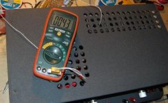
I then doubled the load to 2A, by halving the load impedance to 16 ohms. I left that for more than 15 minutes and the temp went up to 54*C and held. Temp probe was as close to the back of the transistor as possible and touching the heatsink. Both sinks were the same temp, so I'm getting good load sharing and there was no notable voltage drift at the output.
Good stuff!
I ran the supply drawing 500mA for one hour with the cover on. The dummy load for this test is the 32 ohm section of the internal load array that is also inside the case. Temp went from ambient (~24*C) to 43*C in about 10 minutes and it didn't increase at that load:

I then doubled the load to 2A, by halving the load impedance to 16 ohms. I left that for more than 15 minutes and the temp went up to 54*C and held. Temp probe was as close to the back of the transistor as possible and touching the heatsink. Both sinks were the same temp, so I'm getting good load sharing and there was no notable voltage drift at the output.
Good stuff!
Is that ~100% overshoot in the transient response?Transient response:
View attachment 200583
I believe I have it nailed. No oscillation, no output ripple.
Mission accomplished
Is that ~100% overshoot in the transient response?
More than likely some of it is glare or light 'smear' in the photo - look at the 20MHz bandwidth limit symbol in the centre of the display to see what I mean.
I sacrificed better transient response when I added the 100uF cap to the output. See post #122 for a look at the response without the 100uF cap.
Overshoot is normal and unavoidable in any power supply and I think this one would be within the average range.
Is that ~100% overshoot in the transient response?
100% of what? It's just 0.1% of the output voltage.
You can see that the output resistance of about 30 milliohms, assuming it was taken for a load change between 0.5A and 1A. The short blips you see may be further unloading/loading transients going beyond that value but it's hard to see with that timebase setting. They are the reason you usually want capacitors with lowish ESR on the output.
MJL21193, I'm glad that I could help! 😀 I don't see what you mean by that the capacitors made the load transient response worse though. Your first scope shot shows that the initial overshoot was decreased by about ten times. The slow loop response made it look pretty strange afterwards but it still had less maximum deviation from the set value than without the capacitor.
edit: I see you were referring to another post. There doesn't seem to be much difference any longer because the output resistance dominates the response. If you have very high DC gain though you get a response like the attached diagram where the amplitude of the loading/unloading pulses is the load current step size times the ESR of the output capacitor(s).
Attachments
Last edited:
I laid out and made a new board for the digital pot. It is a tiny daughter card that joins with the main board.
Here it is on the right standing up:
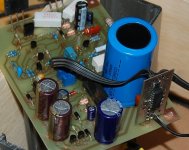
I salvaged everything from the other board, including the 14 pin NAND gate. To remove it, I didn't attempt to desolder it, I just ground down the pins, solder and traces off the bottom of the board and it easily came out without ruining it.
I had thought about surface mounting DIPs before; many times I'll find some useful IC soldered into the board of an old piece of equipment. The problem is always getting it out without cooking it. So I took this as my opportunity to give my idea a try.
Basically, on the board layout I just swapped layers for the component, putting it on the bottom. I moved the pads out and made them solid. The idea is to bend the pins on the DIP so that they go out and flat, like this:
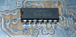
I then soldered it on, just like a surface mount device.
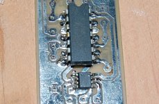
The first one is complete and works perfectly. I used more robust ribbon cable this time and it isn't snaking all over the place.
Here it is on the right standing up:

I salvaged everything from the other board, including the 14 pin NAND gate. To remove it, I didn't attempt to desolder it, I just ground down the pins, solder and traces off the bottom of the board and it easily came out without ruining it.
I had thought about surface mounting DIPs before; many times I'll find some useful IC soldered into the board of an old piece of equipment. The problem is always getting it out without cooking it. So I took this as my opportunity to give my idea a try.
Basically, on the board layout I just swapped layers for the component, putting it on the bottom. I moved the pads out and made them solid. The idea is to bend the pins on the DIP so that they go out and flat, like this:

I then soldered it on, just like a surface mount device.

The first one is complete and works perfectly. I used more robust ribbon cable this time and it isn't snaking all over the place.
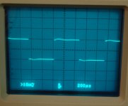
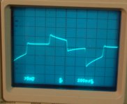
New problem. For some reason, this is what I'm getting back through the wiper of the digital pot:
Here is the schematic:
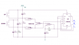
Basic operation: U1A and U1B debounce the switches. U1C, R3 and C4 form a Schmitt trigger oscillator that starts when either switch is held in the 'on' position.
When the DOWN button is pushed, U1B goes low, pulling down the U/D pin of U3. It also pulls the output of U1C low, and the INC pin of U3. The wiper decrements.
When the UP button is pushed, the U/D pin of U3 stays high while the output of U1C goes low, thus incrementing the wiper.
I'm at a loss as to why I'd be getting that back through the wiper. It almost looks like it is stepping 2 up and 2 down over and over.
The data sheet for the pot: X9319

Here is the schematic:

Basic operation: U1A and U1B debounce the switches. U1C, R3 and C4 form a Schmitt trigger oscillator that starts when either switch is held in the 'on' position.
When the DOWN button is pushed, U1B goes low, pulling down the U/D pin of U3. It also pulls the output of U1C low, and the INC pin of U3. The wiper decrements.
When the UP button is pushed, the U/D pin of U3 stays high while the output of U1C goes low, thus incrementing the wiper.
I'm at a loss as to why I'd be getting that back through the wiper. It almost looks like it is stepping 2 up and 2 down over and over.
The data sheet for the pot: X9319
Last edited:
- Status
- Not open for further replies.
- Home
- Amplifiers
- Power Supplies
- Lab Power Supply Design / Build
