I have run 1,000 simulations and yes there are oscillations. Very hard to control. It depends where they come from. If however you are talking about ripple then of course there will be a ripple shape at the output, and you'd need to trace it to the source(s). it may be for example you're drawing too much power out of the transformer, or the filter caps are too low and the base ripple level touches the output level creating kinks... Also the quality/stability of the voltage feeding the base is important. If I remember correctly you are feeding the pass transistors from some rudimentary voltage with no regulation.
I have run 1,000 simulations and yes there are oscillations. Very hard to control. It depends where they come from. If however you are talking about ripple then of course there will be a ripple shape at the output, and you'd need to trace it to the source(s). it may be for example you're drawing too much power out of the transformer, or the filter caps are too low and the base ripple level touches the output level creating kinks... Also the quality/stability of the voltage feeding the base is important. If I remember correctly you are feeding the pass transistors from some rudimentary voltage with no regulation.
Honestly, if this is your best assessment of the circuit and the data I just presented, please save it.
You obviously don't get it.
I'd rather suspect a problem with the voltage regulation loop than your current limiter. It looks like the global loop crossover frequency is as low as about 25 kHz so I'd suspect local oscillation. Perhaps it's the three transistors in the regulation circuit that are acting up in their local loop through the global loop compensation network. It could also be the darlington output stage that dislikes the 10 nF capacitor across the output.
I'd probably redo the voltage loop compensation to go to the base of the "VAS" transistor instead of the LTP input to make sure the regulation circuit itself is well behaved and make the loop crossover frequency a couple of hundred kHz.
It may also be easier to get the thing stable if you use an electrolytic capacitor on the output. A couple of hundred microfarads is often used. As long as the ESR zero (at a couple of tens of kHz) is well below the loop crossover frequency it should be very stable and have low output impedance up to high enough frequencies that it won't matter any more.
BTW, did you set your scope Y amplifier to variable uncalibrated gain on purpose? I've got it's 150 MHz little brother 2445 here. These are pretty nice instruments!
edit: I worry a little that the current sharing of the output stage may not be too stable. It looks like you have your two parallelled output transistors on different (and pretty small) heatsinks and also have small emitter resistors. I fear it could run away to a situation where one transistor does all the work at low output voltages and mid to high current. Do you know the thermal resistance of your heatsinks when mounted in the box that way? The stability can be calculated. If you want to just try it be ware that it could take a pretty long time for the instability to develop.
Last edited:
I'd rather suspect a problem with the voltage regulation loop than your current limiter.
It may also be easier to get the thing stable if you use an electrolytic capacitor on the output. A couple of hundred microfarads is often used.
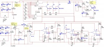
Ok, I tried several things - first I'll re-post the schematic so as we will know what I'm talking about:

I changed C7 to 1nF - slight improvement. I dicked around some with other things then I changed C2 to 1nF(this is big, I know but I wanted to be sure) - bigger improvement, nearly gone. I then added a 220uF electro to the output and viola! Is gone!
So, here is the output with no load at 15VDC:

And here is the output with a load drawing 1.8A at 15VDC:

Did someone say ripple?
If I remember correctly you are feeding the pass transistors from some rudimentary voltage with no regulation
BTW, did you set your scope Y amplifier to variable uncalibrated gain on purpose? I've got it's 150 MHz little brother 2445 here. These are pretty nice instruments!
TBH I don't know what I have going on with that scope - it's been nearly a year since I used it and I haven't had a chance look it over yet.
Yes, it is a pretty good scope and it didn't cost a fortune - a good deal actually.
I worry a little that the current sharing of the output stage may not be too stable. It looks like you have your two parallelled output transistors on different (and pretty small) heatsinks and also have small emitter resistors. I fear it could run away to a situation where one transistor does all the work at low output voltages and mid to high current. Do you know the thermal resistance of your heatsinks when mounted in the box that way? The stability can be calculated. If you want to just try it be ware that it could take a pretty long time for the instability to develop.
So far, the current sharing seems fine and I have had these sinks hot. With the cover on, it may get a little too warm but I'll keep my eye on that. The case has holes in the bottom under the sinks and the cover has holes directly above. It'll have a bit of a chimney effect, some convection to speed cooling.
If need be, I have space between the sinks and the back panel for a pair of muffin fans. Last resort though - that scopes fan is loud enough without adding another 2.
By popular demand, another look. Less blurry pics and a bigger hoop to jump thru
Got to try out the internal dummy load as well.
30VDC output, no load:

30VDC output, 16 ohm load (~1.8A):

The subject:

This is outstanding IMO. I really couldn't have hoped for better.
Ripple is non-existant.
Ultra low noise.
Next to no voltage drop with the load connected.
Sweet!
PS: Thank you Mega for your very effective help - you saved me again!
Got to try out the internal dummy load as well.
30VDC output, no load:
30VDC output, 16 ohm load (~1.8A):
The subject:
This is outstanding IMO. I really couldn't have hoped for better.
Ripple is non-existant.
Ultra low noise.
Next to no voltage drop with the load connected.
Sweet!
PS: Thank you Mega for your very effective help - you saved me again!
Last edited:
Extras, in case someone out there in TV land thinks my scope doesn't discern ripple.
Output of the doubler supply, NO load on output:

Note the v/div.
Output from the raw supply (at the main smoothing cap) with a load - 30VDC @ 1.875A:

I measured voltage drop with the load connected - it went from 30.29V to 30.13V. Not too shabby.
Output of the doubler supply, NO load on output:
Note the v/div.
Output from the raw supply (at the main smoothing cap) with a load - 30VDC @ 1.875A:
I measured voltage drop with the load connected - it went from 30.29V to 30.13V. Not too shabby.
Do you really want the weak foldback characteristic given by R21 or is it perhaps tuned to counteract the early effect in the current limit transistor?
Going back to this from page one, I'm beginning to wonder if this is the cause of the instability. Looking at the function, R21 serves 2 purposes: First it (along with R20) provides a dummy load for the output so that it can be adjusted down to zero. Second, it supplies positive feedback to the emitter of Q6. The reason for this is that when in constant current mode (current limiting), as the output voltage falls the additional drive necessary to turn on Q6 harder is supplied via its emitter, through R21. This prevents an increase in output current.
I will have to investigate further.
Another thought: while added to improve stability, what does the 220Uf cap across the output do to the transient response? Is transient response a critical factor for a supply like this? I could rig up something to measure it - a couple of resistor loads and a MOSFET to switch one in parallel with the other, thereby switching the current draw from low to high. This could be driven with a squarewave from my FG. Maybe I'll give it a try.

The rig:

With the 220uF cap:

Without the cap:

I see no signs of oscillation with the cap removed now. I did make one subtle change this morning - I added a 470 ohm resistor in series with pot P_R19 to stop it from hitting 0 volts. This seemed to trigger oscillation before.
As for the transient response - I think that I need to go back 'in' and fine tune the compensation caps that I replaced last night in order to stabilize the supply. The one in the CV loop in particular.
With the 220uF cap:
Without the cap:
I see no signs of oscillation with the cap removed now. I did make one subtle change this morning - I added a 470 ohm resistor in series with pot P_R19 to stop it from hitting 0 volts. This seemed to trigger oscillation before.
As for the transient response - I think that I need to go back 'in' and fine tune the compensation caps that I replaced last night in order to stabilize the supply. The one in the CV loop in particular.
Much trial and error later, it seems I have the stability problem sorted out. I found that a cap (ideal value yet to be determined) from the base of Q5 to '0' volts most effectively tamed the oscillation. It seems that it was indeed the 'VAS' (as Mega called it, it actually sinks current from the base of Q1 to regulate the output voltage) that was responsible.
As well:
Curious if it matched the simulation results and in response to this comment (again):

Take note of the V/div scale. (~23mVpp)
I then scoped immediately after R1 (what drives the base of Q1):

note the V/div scale again, same time base (less than .2mVpp). Interestingly enough, this is free of ripple. This is (nearly) as clean an a pure DC source.
The same, but with a load at the supply output drawing 1.2A:

Virtually unchanged. There is no ripple of any significance.
This result is not obvious at first glance. After all, we expect huge ripple from a relatively unfiltered and unregulated doubler supply, and would think it would make for a pretty rough base supply for a regulators pass transistor. TBH, I was very surprised when I saw this in simulation and I felt that it could not be a true representation of real world operation. It in fact was an accurate prediction of the outcome, as shown in the actual scope shots above.
As well:
Curious if it matched the simulation results and in response to this comment (again):
I did some more measuring. I scoped the output of the doubler supply again, before R1:If I remember correctly you are feeding the pass transistors from some rudimentary voltage with no regulation
Take note of the V/div scale. (~23mVpp)
I then scoped immediately after R1 (what drives the base of Q1):
note the V/div scale again, same time base (less than .2mVpp). Interestingly enough, this is free of ripple. This is (nearly) as clean an a pure DC source.
The same, but with a load at the supply output drawing 1.2A:
Virtually unchanged. There is no ripple of any significance.
This result is not obvious at first glance. After all, we expect huge ripple from a relatively unfiltered and unregulated doubler supply, and would think it would make for a pretty rough base supply for a regulators pass transistor. TBH, I was very surprised when I saw this in simulation and I felt that it could not be a true representation of real world operation. It in fact was an accurate prediction of the outcome, as shown in the actual scope shots above.
Last edited:
Sorry my bad choice of words keeps appearing all the time, I do not know where to hide
What I was saying in that statement is that the pass transistors are fed a very impure signal with ripple as you saw on the scope.
The diff amp is a monitor, it always senses the output voltage and tries to keep it constant through Q5. If the output voltage increases for some reason, any reason, it will open Q5 more, and the other way round. This is all reactive.
The transistor Q5 opens and closes all the time in unison with the ripple coming through R1 (and other factors) to keep the base voltage constant.
Actually Q5 is the instrument in the hands of the op-amp (the differential amp) which senses the voltage output and tries to keep it stable. This nullifying of the ripple at R1 is not perfect and some will feed through and show on the scope (on simulation at least, with some very little V/div). Same applies with ripple arriving at the collector and with load changes at the emitter of the pass transistors.
The diff amp / Q5 combo has to fight against all these:
(a) ripple through R1
(b) ripple and voltage changes at the collector of the pass transistors (the more current you draw the greater the ripple)
(c) spontaneous changes at the emitter of the pass transistors (when the load changes, as your test with that square wave showed).
As I tested in simulation, the way the diff amp reacts to changes in the output voltage (which tries to keep constant) is the key, because if it is too slow then you will get waves at the output, and if it is too quick then you will get oscillations (eg if you replace the diff amp with a comparator). I found out, what works best is an op-amp/diff amp with a gain of about 10x-15x and adequate HF compensation and negative feedback.
It seemed to me at the time when I was experimenting with similar circuits (on the simulator) that I could help the diff amp to do its job as much as I could, by trying to eliminate/reduce (a) and (b).
However, you have practically proven that you can almost throw the kitchen sink at the output voltage and the diff amp/Q5 will keep it almost perfectly smooth.
However, you have practically proven that you can almost throw the kitchen sink at the output voltage and the diff amp/Q5 will keep it almost perfectly smooth.
And this, IMO, is the absolute beauty of this method. It is simple and elegant.
The first objective to to have a stable output voltage that is minimally affected by load - this has been met.
The second objective is to have minimal ripple at the output, regardless of load conditions - this has been met.
Paramount is stability IMO, and this caused me much concern. Getting the supply to a stable operating condition was something I should have done in the prototype stage. The fact is, I didn't do enough testing, wanting to hastily bull ahead (born in May BTW
). There are lessons to be learned in every project and this one taught me a lot, especially to slow down and 'throw the kitchen sink at it' during the prototyping.PS: Sorry if I came off a bit harsh earlier. Sometimes my frustration at a setback bleeds through to the things I 'say'.
(c) spontaneous changes at the emitter of the pass transistors (when the load changes, as your test with that square wave showed).
This is my transient response test and it puts a switching impedance on the output of the supply - 36 ohms and 18 ohms. The rig (shown in post #111 and 112) does this and IT is driven from a squarewave output from my function generator. This doubles the load at each cycle (if testing at 1khz, it would switch 1000 times per second) and shows how quickly the supply copes with load changes.
To stabilize the supply, I put a cap from the base of Q5 to 'ground'. I went for broke here and put a 1uF cap, just to see if it would halt the oscillation. It did and before I do more testing to see if a smaller value will work, I ran the transient response test again.
This is the result:

This is at ~1KHz. As can be seen this response is much improved over the previous runs and I'm tempted to leave things as they are. The response is free of the over-damped compensation effects shown earlier.
Last edited:
You should turn those VAR controls coming out of the middle of the volts/div selectors fully clockwise until they click into the calibrated position. The > symbol to the left of the sensitivity readout means the sensitivity of the oscilloscope is turned down from its calibrated value.
The ripple looks pretty good but the transient response is a little slow compared to what is possible. But if you are content with it then I guess it needs no bettering, of course. I'd use standard miller compensation around Q5, probably with a resistor in series like you have now to get sensible components values for a nice loop crossover frequency. The current R3 does not do much though. It won't have much effect until about two decades above the loop gain crossover frequency.
A large output capacitor is often used because it helps the transient response but if it's too large the protection of the current limit is reduced because a lot of energy is stored in it. My Hewlett Packard 0-50 V, 0-10 A (but limited to 200W too) power supply actually has about 3000 µF of output capacitance if I remember correctly!
You should turn those VAR controls coming out of the middle of the volts/div selectors fully clockwise until they click into the calibrated position. The > symbol to the left of the sensitivity readout means the sensitivity of the oscilloscope is turned down from its calibrated value.
When I bought the scope, I asked the seller if it was recently calibrated. He said that it has a calibration seal and a sticker showing calibration by Agilent in 2006. I figured it couldn't be that far off so I bought it.
I searched online for a manual (it didn't come with one) and I found a calibration guide issued for the US Army. I used that to quickly check things over and saw that it is out of calibration and at the time I calibrated (by use of the VAR knob) the vertical amp to a very close setting (I'm not designing nuclear clocks here, so that would be close enough).
While looking at the ripple at the 2mV scale, I forgot my 'calibration' and turned the VAR knob to get a better look. Ooops.
I've since re-calibrated it back to 'normal'.
The ripple looks pretty good but the transient response is a little slow compared to what is possible. But if you are content with it then I guess it needs no bettering, of course. I'd use standard miller compensation around Q5, probably with a resistor in series like you have now to get sensible components values for a nice loop crossover frequency. The current R3 does not do much though. It won't have much effect until about two decades above the loop gain crossover frequency.
A large output capacitor is often used because it helps the transient response but if it's too large the protection of the current limit is reduced because a lot of energy is stored in it. My Hewlett Packard 0-50 V, 0-10 A (but limited to 200W too) power supply actually has about 3000 µF of output capacitance if I remember correctly!
Funny, I attributed the poor TR in post #112 to the 220uF cap. I'll try it again.
As for compensation, I'm open to suggestions. At this point, I'm going to get ALL of the bugs worked out before proceeding. When I'm absolutely satisfied that everything is A-OK, I'll make NEW boards (again!), including all of the changes/refinement. I also want to include the digital pots on the supply board - slivers of hard-wired ribbon cable running here, there and everywhere is no good.
I am not sure about the cap on Q5, I would think Q5 needs to be quick to react when it receives an order from the diff amp. Maybe the diff amp needs a cap here and there in its feedback loop? On my simulation I used 1nF negative feedback on the voltage regulator op-amp and 10X gain.
One more thing, you may want to put a 22uF-47uF cap at the ADJ pin of the LM317, as per manufacturer instructions to eliminate ripple from the reference voltage and from the diff amp.
I attach my almost final schematic so you can see the similarities and differences. I use a separate supply to power the op-amps and again a separate zener to feed the pass transistors' bases and again a separate zener to provide the voltage reference and finally another zener to provide the reference for the current limiter. Lots of zeners
Attachments
One more thing, you may want to put a 22uF-47uF cap at the ADJ pin of the LM317, as per manufacturer instructions to eliminate ripple from the reference voltage and from the diff amp.
Ahead of you there:

You have been busy, I see. I'll take a closer look.
You are using MS. If you don't mind, can you attach it? Just change the extension to .txt
Last edited:
- Status
- This old topic is closed. If you want to reopen this topic, contact a moderator using the "Report Post" button.
- Home
- Amplifiers
- Power Supplies
- Lab Power Supply Design / Build