how did your project go? I have similar speakers B&W CM8 and considering using L20 V 9.2 boards.
I suggest you use l20v10
Green version.
Attachments
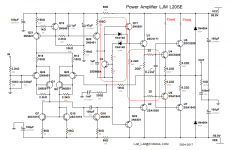
LJM L20SE Design Notes
LJM L20SE Design Notes (*)
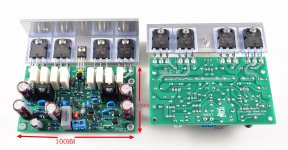
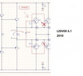
1. The amplifier is built on a green PCB with approximately 110 x 50 X 40 mm (LxWxH).
2. The audio signal first passes R1/C1 which form a first-order input low-pass filter that keeps out unwanted radio frequencies. R2 provides a return path for the input bias current of the amplifier’s input stage (note that the value of R2 is set to equal that of R14 so that voltage drops across these two resistors balance out any DC offset). The signal then reaches transistor Q2, which forms a differential amplifier input stage with Q3. It is fed a constant current from the constant current source (CCS) Q8/Q1/R3. Q4 and Q5 cascode the differential stage. They keep the heat power loss low and provide for low input capacitance and high bandwidth. Towards the negative supply line follows a current mirror comprised of Q6/R8/Q7/R9. It guarantees for good symmetry, high openloop gain and low sensitivity against disturbances on the supply rail (PSRR).
3. Q10 forms the voltage amplifying stage (VAS) that works on the CCS-connected Q9 as load. Between Q10 and Q9 we find the biasing network Q11/R17/R18/C8 that generates and regulates the bias voltage for the output stage.
4. R14 and R15/C3 define the amplification factor. The large capacitor C3 improves offset accuracy by reducing the closed-loop gain to unity at DC. That spares the use of an active DC-servo stage and functions rather well under most circumstances.
5. C5 is connected across Q10’s collector and base as a compensation cap to limit Q10 gain at high frequencies (Miller Effect).
6. The driver transistors Q12/Q14 and Q13/15 Darlington drive the power transistors Q16/Q18 and Q17/Q19. The bases of Q14 and Q15 are connected together by R23.
7. The power transistors are connected to the speakers by means of the R24/R26 and R25/R27 damper-resistors.
8. At the output we find a R28/C11 Zobel network (the R28 10 Ohm approximates to the expected loudspeaker load impedance and the C11 capacitor is invariably 100 nF) to mitigate amplifier high frequency instability due to loudspeaker voice-coil inductive reactance.
9. The diodes D3 and D4 are “catcher-diodes”, i.e., they have a dual purpose: they protect from accidental power supply reverse polarity and they also protect the amplifier from loudspeaker inductive loads that can push energy back into the amplifier output, resulting in a possible rise of the output voltage above the supply rails and possible destruction of the output transistors due to polarity reversal. These diodes catch away the overvoltage to their maximum forward voltage (hence the term catcher-diode).
(*) Based on Calvin’s work: L12-2, powerful, good, low-cost - calvins-audio-pages
J.A.
LJM L20SE Design Notes (*)
1. The amplifier is built on a green PCB with approximately 110 x 50 X 40 mm (LxWxH).
2. The audio signal first passes R1/C1 which form a first-order input low-pass filter that keeps out unwanted radio frequencies. R2 provides a return path for the input bias current of the amplifier’s input stage (note that the value of R2 is set to equal that of R14 so that voltage drops across these two resistors balance out any DC offset). The signal then reaches transistor Q2, which forms a differential amplifier input stage with Q3. It is fed a constant current from the constant current source (CCS) Q8/Q1/R3. Q4 and Q5 cascode the differential stage. They keep the heat power loss low and provide for low input capacitance and high bandwidth. Towards the negative supply line follows a current mirror comprised of Q6/R8/Q7/R9. It guarantees for good symmetry, high openloop gain and low sensitivity against disturbances on the supply rail (PSRR).
3. Q10 forms the voltage amplifying stage (VAS) that works on the CCS-connected Q9 as load. Between Q10 and Q9 we find the biasing network Q11/R17/R18/C8 that generates and regulates the bias voltage for the output stage.
4. R14 and R15/C3 define the amplification factor. The large capacitor C3 improves offset accuracy by reducing the closed-loop gain to unity at DC. That spares the use of an active DC-servo stage and functions rather well under most circumstances.
5. C5 is connected across Q10’s collector and base as a compensation cap to limit Q10 gain at high frequencies (Miller Effect).
6. The driver transistors Q12/Q14 and Q13/15 Darlington drive the power transistors Q16/Q18 and Q17/Q19. The bases of Q14 and Q15 are connected together by R23.
7. The power transistors are connected to the speakers by means of the R24/R26 and R25/R27 damper-resistors.
8. At the output we find a R28/C11 Zobel network (the R28 10 Ohm approximates to the expected loudspeaker load impedance and the C11 capacitor is invariably 100 nF) to mitigate amplifier high frequency instability due to loudspeaker voice-coil inductive reactance.
9. The diodes D3 and D4 are “catcher-diodes”, i.e., they have a dual purpose: they protect from accidental power supply reverse polarity and they also protect the amplifier from loudspeaker inductive loads that can push energy back into the amplifier output, resulting in a possible rise of the output voltage above the supply rails and possible destruction of the output transistors due to polarity reversal. These diodes catch away the overvoltage to their maximum forward voltage (hence the term catcher-diode).
(*) Based on Calvin’s work: L12-2, powerful, good, low-cost - calvins-audio-pages
J.A.
Attachments
Hello everyone.
I have issue with my L20SE (board looks like at post #44 this thread).
At input signal 1 kHz 100 mV and output signal near 2 V, amplifier consumes approximately 2.3 A on each rail.
There is no more than 20 mA consumption without input signal.
PSU output is +-45 V.
Loading resistor is 47 Ohm.
Output signal without distortion and DC.
What a problem can it be?
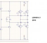
I looked at the diagram and was a little surprised, because. the Lokanti output stage is completely organized, the reason is the weak current of the drivers U1 and U2, resistors are also needed in the bases of the output stages and capacitance between the bases to speed up the recharging of the base currents of the output transistors when they work in class AB.
Also, the Bailey multiplier is completely incorrectly organized, first of all, you need to remove the 33kΩ resistor, because. supply ripples flow through it to the input of the output stage, and the circuit itself is organized as in the picture I presented, it will not be difficult to select resistors in the base of the multiplier for the no-load current of the output transistors equal to 75mA per pair ...
see Attachment.
Miller correction can be left on for now, although a better sound can be obtained with progressive correction.
Attachments
L20v6 uses your circuit. L20v9.2 does not use your connection.I looked at the diagram and was a little surprised, because. the Lokanti output stage is completely organized, the reason is the weak current of the drivers U1 and U2, resistors are also needed in the bases of the output stages and capacitance between the bases to speed up the recharging of the base currents of the output transistors when they work in class AB.
Also, the Bailey multiplier is completely incorrectly organized, first of all, you need to remove the 33kΩ resistor, because. supply ripples flow through it to the input of the output stage, and the circuit itself is organized as in the picture I presented, it will not be difficult to select resistors in the base of the multiplier for the no-load current of the output transistors equal to 75mA per pair ...
see Attachment.
Miller correction can be left on for now, although a better sound can be obtained with progressive correction.
L20v9.2 performance is improved. Instead of declining.
The early version of L20 is the same as your circuit.
L20se= l20v9.2, only 2 pairs of transistors are reduced
The high frequency performance of l20se or l20v9.2 has been greatly improved.
Maybe in practical application. That capacitor will leak electricity. But in the ideal state, there is no problem.
In fact, we need to know. Many theories. Just theory.
The same circuit. Different components. It's completely different. Measurement is only used in practical applications.
Only then can we know the result. Just read the circuit information on the Internet. In fact, it can't be judged.
I even found many measurement results. It is also incorrect.
But I can communicate with you. It's a very pleasant thing. I hope to continue the discussion if possible.
Attachments
Last edited:
Like this correct as in attachment.
the reasons are as follows:
1. C13 in your version gives an additional capacitive load to the Q12Q13 driver, so it must be moved to the base of the output stage transistors so that it accelerates the recharge of the base capacitances of the output transistors Q14-Q17 there/
2. you should not add a resistor to the base each transistor when connecting the output transistors in parallel - this increases the input capacitance of the entire parallel cascade and slows down its recharge, it is enough to connect one resistor and the base of the output transistors to one point after this resistor.
Attachments
Last edited:
.. Many theories. Just theory....
no theories, only practically correct implementations.
as Douglas Self said, a lot of audio consists of false statements.
P.S. square wheels can be screwed to the bike, but it is still better when the wheels are round ....
Last edited:
I'm glad to discuss this.no theories, only practically correct implementations.
as Douglas Self said, a lot of audio consists of false statements.
P.S. square wheels can be screwed to the bike, but it is still better when the wheels are round ....
But what you said. I have tried almost all of them.
in fact. These things are not so important, whether you say it or I say it.
In addition, I would like to add. I made the self circuit directly. But in fact, there is something wrong with the circuit of self. It's not stable. I've changed it. After more than ten years of use. There was no problem.
I understand that someone will have questions about the circuit,
If you are interested, I can email you l20se design drawings.
I can also measure your plan. LJM_LJM@FOXMAIL.COM
But I personally don't think these are particularly important changes. I am more concerned about the impact of output structure.
Attachments
The Lokanti output stage has the lowest distortion to date and is therefore only used in high level audio. In fact, there is only one option for the practical implementation of this scheme, there is nothing to invent and think over, you just need to apply it and that's it ...
I am so sorry, that you have been using a current starvation driver for output transistors for 10 years, because a transistor is a current element, it can give as much current to the load as it can take from the previous stage, multiplied by the transfer coefficient, and the previous stage should always stay in class A.
Ок, my mail: Hennady@ukr.net
I can understand what you mean.The Lokanti output stage has the lowest distortion to date and is therefore only used in high level audio. In fact, there is only one option for the practical implementation of this scheme, there is nothing to invent and think over, you just need to apply it and that's it ...
I am so sorry, that you have been using a current starvation driver for output transistors for 10 years, because a transistor is a current element, it can give as much current to the load as it can take from the previous stage, multiplied by the transfer coefficient, and the previous stage should always stay in class A.
Ок, my mail: Hennady@ukr.net
In fact, I had the same doubts ten years ago. If you add a resistance to the first stage drive.
Make them work in class A. But later I studied the design scheme of the most powerful analog circuit company in the world. Don't doubt it. It is indeed the most powerful analog circuit company in the world.
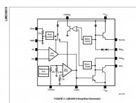
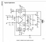
That is, the national semiconductor company's product LME49810.
So I get inspiration from its chip scheme. Then carry out the test.
If you are interested. Carefully study the drive circuit of LME49810 and you will find
It is exactly the same as l20se.
And after my measurements, I found
L20se has the same performance index as LME49810 at the output stage.
It's very good. So I gave up the circuit architecture of self.
Attachments
Yes,I can understand what you mean.
....
If you are interested. Carefully study the drive circuit of LME49810 and you will find
It is exactly the same as l20se.
...
firstly, where the microcircuit shows a source of stable current, you have a 33 kOhm resistor,
secondly, two darlington junctions are shown, this does not quite mean that a darlington with current starvation of the driver should be installed,
thirdly, the maximum load of 8 ohms is indicated - many high-quality the speakers have dips in the complex impedance rating of up to 2.7 ohms, a Darlington with current starvation simply physically will not have anywhere to get additional current for a high-quality current surge into the load ...
Sorry, but I think that such a repetition is not entirely justified ... it doesn't come close to a quality audio power amplifier...
In fact, l20se is a three-level EF output.Yes,
firstly, where the microcircuit shows a source of stable current, you have a 33 kOhm resistor,
secondly, two darlington junctions are shown, this does not quite mean that a darlington with current starvation of the driver should be installed,
thirdly, the maximum load of 8 ohms is indicated - many high-quality the speakers have dips in the complex impedance rating of up to 2.7 ohms, a Darlington with current starvation simply physically will not have anywhere to get additional current for a high-quality current surge into the load ...
Sorry, but I think that such a repetition is not entirely justified ... it doesn't come close to a quality audio power amplifier...
Its current amplification ability is its advantage.
There is no problem when the output exceeds 10A.
Only the driver does not work in class A. But it has no high-frequency distortion. Even reduce high-frequency distortion.
Because it can be tested or listened to. High frequency is great.
So thank you again for your advice. I will still send you an email. Then measure your plan. But I did use the same structure you said before. L20 V6。 But it doesn't prevent me from entering again
by itself, this parameter does not make sense, because the maximum current at which the output stage remains in linear mode is important, which is why all high-end amplifiers are made with a large number of parallel output transistors.....
There is no problem when the output exceeds 10A.
...
it is practically impossible to get more than 2A in the AB class from one pair in linear mode, so I will ignore the value you specified in 10A ...
The output current can be easily calculated.by itself, this parameter does not make sense, because the maximum current at which the output stage remains in linear mode is important, which is why all high-end amplifiers are made with a large number of parallel output transistors.
it is practically impossible to get more than 2A in the AB class from one pair in linear mode, so I will ignore the value you specified in 10A ...
Can't you count it. Theoretically, it can exceed 15 -20a.
Your method is wrong. This is very simple. Voltage amplification stage current X nno1, no2, no3 hfe
Output stage The output current has nothing to do with the static working current.
Lm4702 and LME49810 have the same structure.
You can send an email to National Semiconductor Corporation. Tell them the wrong circuit.
Last edited:
Why be rude?The output current can be easily calculated.
Can't you count it. Theoretically, it can exceed 15 -20a.
Your method is wrong. This is very simple. Voltage amplification stage current X nno1, no2, no3 hfe
Output stage The output current has nothing to do with the static working current.
Lm4702 and LME49810 have the same structure.
You can send an email to National Semiconductor Corporation. Tell them the wrong circuit.
it is very easy to calculate the current, for example, for 10A in a 4Ω load, an output power of 625 watts is needed (for one pair of output transistors it’s a bit too much), which will make the amplitude voltage Vp = 62.5 volts, because in your circuit, the current of the voltage amplifier driver is limited by the initial current, then this is not rail to rail voltage, but about 60% of the supply voltage, i.e. to get 10A in linear mode you need +/-105 volts bipolar supply.
....Theoretically, it can exceed 15 -20a....
yes, that's right, this is meant for the peak signal factor, the instantaneous maximum value and has nothing to do with the linearity index of the system ...
You may have misunderstood again.Why be rude?
it is very easy to calculate the current, for example, for 10A in a 4Ω load, an output power of 625 watts is needed (for one pair of output transistors it’s a bit too much), which will make the amplitude voltage Vp = 62.5 volts, because in your circuit, the current of the voltage amplifier driver is limited by the initial current, then this is not rail to rail voltage, but about 60% of the supply voltage, i.e. to get 10A in linear mode you need +/-105 volts bipolar supply.
Current is not only related to voltage. It is also related to resistance.
So what you said. Not exactly. You have to trust me. I understand everything you said.
But in fact, I don't think there is much difference between the two.
In fact, there is no so-called linearity in transistors. It is the standard Darlington structure.
If you think that Darlington structure cannot output relatively large current, it is like saying that 1+1 cannot =1.
I don't think it's wrong for you to stick to your idea. But there is no need to deny that everything else is wrong.
I calculated its current output capacity when I improved the driving circuit of l20v6 and l20v9.2.
In the calculation, I come to the conclusion that they are the same. I hope you can tell me something. Something I don't know.
I understand that you want to say that the secondary drive does not work in class a mode.
But whether it is class A or class B. They output the same current.
If there is no distortion. Or the high-frequency distortion is the same. That makes no difference.

In fact, this kind of circuit has some problems that the voltage width of crossover distortion is larger.
No one may find it. But I found this phenomenon. So if you are interested, you can study how to reduce the crossover distortion of his VBE voltage width.
Last edited:
....
If there is no distortion. Or the high-frequency distortion is the same. That makes no difference.
In fact, this kind of circuit has some problems that the voltage width of crossover distortion is larger.
No one may find it. But I found this phenomenon. So if you are interested, you can study how to reduce the crossover distortion of his VBE voltage width.
The reason for the occurrence of crossover distortion is the different slope of the transmission characteristics of output complementary transistors. They can be reduced by current control of the output stage, but Miller's correction imposes restrictions on such a solution. If you want to get rid of crossover distortion, you will have to get rid of Miller correction.
the second problem is the thermal distortion of the output transistors, which leads to the formation of parasitic frequency modulation. the speed qualities of the same transistor with different crystal temperatures are not the same, and this is also very noticeable in the output transistors.
the solution here is to use the Lokanti topology, because the bulk of the signal amplification work moves from the output stages to the driver stages, which operate at lower currents and lower temperatures and are more symmetrical in characteristics with complementary performance than high-power output transistors ...
- Home
- Amplifiers
- Solid State
- L20 AMP。use only two NJW0302G