Mark A. Gulbrandsen said:Q-111
E -1.06
B -.563
C +1.296
Terry,
these are the numbers Mark measured for the 2SC3955.
The E value should be -1.296 V, (same as B value Q110), then the -0.563 value on the B makes sense.
Means the voltagedrop from the base to the emitter of that device is 0.733 volts.
If you are using the same values :
R124 = 4700 R
R125 = 820 R
R126 = 5000R trimmpot,
then the trimmpot turned to maximum resistance should give you ~1.33 volts across the 2SC3955, in minimum resistance setting ~ 4.93 volts.
On the outputs after the drivers on the main board you should be getting between +/- 0.1 and +/- 1.9 volts when you turn the trimmpot.
(you should start adjusting the bias with the trimmpot in maximum resistance setting, with all of the cutting of those boards i would measure which way the trimmpot turns with a DMM first and check its value)
This you can do safely without the outputs connected, in maximum output voltage position the 25 R resistors get less than a 1/10th of their max. power capability
From your posted measurements :
Connected:
Q107 C = + 1.29
Q109 B = + 1.296
Q111 C = + 1.296
Connected:
Q108 C = -1.288
Q110 B = -1.296
Q111 E = -1.06 <== should be -1.296 also
I've received the remaining parts for me Krellster today, i'll post a pic of the junk this evening, then i'll hush and wait for the boards.
Connected:
Q107 C = + 1.29
Q109 B = + 1.296
Q111 C = + 1.296
Connected:
Q108 C = -1.288
Q110 B = -1.296
Q111 E = -1.06 <== should be -1.296 also
I've received the remaining parts for me Krellster today, i'll post a pic of the junk this evening, then i'll hush and wait for the boards.
I measured mine at 43.4 rails and did my best to bias at .4 v across RE1
Mark************************Mine
Q-101
E .745**********************-.544
B 142.9 mv*******************15.2
C +36.07*********************40.1
Q-102
E .442***********************.587
B 143 mv*********************15.2
C - 35.6**********************-40.0
Q-103
E .617***********************.541
B 0*************************15.6
C +35.9********************* 41.2
Q-104
E .320************************.586
B 0***************************15.6
C -35.75**********************-40.0
Q-105
E +36.5***********************40.7
B 35.95***********************40.3
C 0**************************** 0
Q-106
E -36.32**********************-40.7
B -35.7***********************-40.0
C 0*************************** 0
Q-107
E +37.05***********************41.2
B +36.5************************40.7
C +1.29************************1.381
Q-108
E -36.8*************************-41.2
B -36.33************************-40.6
C -1.288************************-1.346
Q-109
E +.728*************************1.01
B +1.296************************1.381
C +38***************************42.4
Q-110
E -.733**************************-.957
B -1.296*************************-1.352
C -37.88*************************-42.3
Q-111
E -1.06*************************-1.346
B -.563*************************-.692
C +1.296************************1.380
+ side OP device
E 120 mv*************************.445
B +.728**************************1.020
C +38.09*************************42.4
- Side OP Device
E 140 mv**************************-.452
B -.733****************************-.967
C -37.89***************************-42.4
OK, please look these over and give me some ideas where I am getting the problems. Obviously my base voltages are off for Q-101,102,103 & 104.
This is on my good board. The other board has some blown resistors. I will probably have to replace all to be sure. If I can get this one straightened out it will help troubleshooting the other.
Thanks, Terry
still4given said:Q-103
E .617***********************.541
B 0*************************15.6
C +35.9********************* 41.2
Q-104
E .320************************.586
B 0***************************15.6
C -35.75**********************-40.0
Howcome you have 15.6 Volt on the input?
Looks like you have a connection between the bases of Q101 to Q104.
Vbe of your drivers is very low at 350-380 mV, they should be near 600 mV, at a higher bias than Mark's their values should be higher than his.
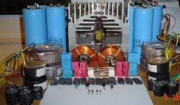
Here is my garbage:
2SA970/2SC2240BL/2Sa968/2SC2238/MJE15032/MJE15033.
I forgot to put the MPSA42/92 with the lot, at the front are the 9vac toroidal step-up transformers for the front end regulation.
+ and - will have separate transformers, 2 300va toroids on each side.
2SA970/2SC2240BL/2Sa968/2SC2238/MJE15032/MJE15033.
I forgot to put the MPSA42/92 with the lot, at the front are the 9vac toroidal step-up transformers for the front end regulation.
+ and - will have separate transformers, 2 300va toroids on each side.
Attachments
Mark A. Gulbrandsen said:Terry,
Did you use the 2SC/2SA semis or the MPS type Motorola-On Semis. The basing is different if you subbed the latter in place.
Mark
Yes, I used the 2sc/2sa just as called out in the BOM.
To be honest, I could be wrong about the voltages I posted. THe voltages are true but I didn't pull up the data sheets for the devices and may have said something was a base when it was a collector. I'm not sure. Tomorrow, I will redo it and try and follow the traces to see which they are. I'm too tired to do anymore tonight. I thought perhaps there was a diode that failed or something. I have no idea how to check a capacitor. It's possible the one of electrolytics got damaged when I had the rails reversed.
Thanks for the help.
Terry
For reference/adding to the wiki the +/- signs for measured voltages need be put on the list correctly.
e.g.:
Q101 and Q103 are NPN devices, current flows from the base into the emitter, emitter voltage is lower than base voltage.
With 0 and +143 mV on the base of Q101/Q103 the E values should have a negative sign.
With 0 volts on the base of Q101 to Q104 1.4 mA should be flowing in the collector of Q101 and 1.4 mA in Q103, corresponds with the voltagedrop over R112/R116 from rails to the +36 volt on the collector side from the measurements.
2 * 1.4 mA * 9150 ohms = less than 27volts, so emitter voltage of Q101/Q103 should be negative.
Setting the Bias
Ok, I'm about to try setting the bias and beginning to reread all the related posts on that topic.
What settings should I have to get 50 W class A into-
4 ohms,
8 ohms
same question for 70W class A into-
4 ohms
8 ohms.
I've got 4 TO3 pairs per channel, 38V rails, .499 ohm 10 W emitter resistors.
Reason I ask is because I've got somewhat oversized fan cooled heatsinks and would like to keep upping the bias (but not too much) to hopefully get a little more performance/bias than the stock KSA-50.
I assume the answer to this can be figured out in the hundreds of posts on the topic which I'm reading tonight, but figured I'd ask anyway.
Also- how many watts does each of the driver transistors dissipate in a worst case scenario? I'm increasing their heat sinking and wondering about this.
For 4 output devices per channel :
50 watts class A :
8 ohm:
1.8 amp bias = 0.9 amp per device= 0.45V across the Re
4 ohm:
2.55 amp bias= 1.275 amp per device= 0.64V across the Re
70 watts class A ;
8 ohm:
2.15 amp bias= 1.075 amp per device= 0.54V across Re
4 ohm:
3 amp bias = 1.5 amp per device= 0.75V across the Re
For 8 devices per channel bias per device is halved, so voltage across Re also halved
jacco vermeulen said:For 4 output devices per channel :
50 watts class A :
8 ohm:
1.8 amp bias = 0.9 amp per device= 0.45V across the Re
4 ohm:
2.55 amp bias= 1.275 amp per device= 0.64V across the Re
70 watts class A ;
8 ohm:
2.15 amp bias= 1.075 amp per device= 0.54V across Re
4 ohm:
3 amp bias = 1.5 amp per device= 0.75V across the Re
For 8 devices per channel bias per device is halved, so voltage across Re also halved
Jacco, the only boards that are currently in the hands of anyone able to ask such a question have 6 output devices as per The original boards.
Anthony
Coulomb said:
Jacco, the only boards that are currently in the hands of anyone able to ask such a question have 6 output devices as per The original boards.
Anthony
That would be if you use the output boards. If you are using TO3 devices you can use more or less since the output boards aren't used.
jacco vermeulen said:For 4 output devices per channel :
50 watts class A :
8 ohm:
1.8 amp bias = 0.9 amp per device= 0.45V across the Re
4 ohm:
2.55 amp bias= 1.275 amp per device= 0.64V across the Re
70 watts class A ;
8 ohm:
2.15 amp bias= 1.075 amp per device= 0.54V across Re
4 ohm:
3 amp bias = 1.5 amp per device= 0.75V across the Re
For 8 devices per channel bias per device is halved, so voltage across Re also halved
Hey jacco,
I am using 3 pair per channel. Are you saying that I should reduce the voltage across the Re by 1/3?
Thanks, Terry
worst case scenario...
Ooh my head, just back from vegas...
The worst case scenario for the transistors depends on a lot of variables, including load impedance, output count, rail voltage, emitter resistors etc.
The 'biggest' limiting case will be when your entire transformer capacity is being used, in which case a rough and ready approximation might be the peak transformer VA divided by 2, spread across the entire set of outputs...though at this current level a chunk of power will be going into the emitter resistors as well...
I don't know if there is a accepted way of determining peak transformer capacity, but I double the nominal rating...the toroids I've tried this on will be fine for many minutes, but eventually they get hot...
Stuart
still4given said:I am using 3 pair per channel. Are you saying that I should reduce the voltage across the Re by 1/3?
Mr Green posed the question for 4 pairs of output devices, thats 8 per channel.
Maybe he meant 4 per channel, so i gave the numbers for either one.
Mr Green posted plenty of sizeable pictures of his NO-output board production.
The bias current divided by the number devices per rail is the biasing current per device.
This number times the Re value is the voltage you measure across 1 output device emitter resistor.
For Mr Green's 0.499 Re's those are the voltages numbers.
If you are using 0.68 ohm Re's you need to multiply this value with the bias per device.
[The output bias needs to be a little higher than the current needed to reach the power number, because at 50(or 70) watts output in class A the devices on the other rail are still a bit opened( in their linear range).
So for 4 devices in parallel instead of 2 the bias actually needs to be a little bit higher than in the case of 2 in parallel]
Maybe a nice one would be to take peak dissipation for the drivers at 20 amps rms in 1 Ohm ?
Hi Terry,
I am going technical on you but stay with me, all you need is a calculator.
Total bias current (Iq) = 1.8A for 50W into 8ohms. Iq = sqrt(P/R/2)
Number of output device pairs = 3
Bias current per pair = 1.8/3 = 0.6A = 600mA
Voltage across a single Re of 0.68ohms is current times resistance,
So Bias voltage (Vre) = I * R = 0.6 * 0.68 = 0.408V = 408mV
Terry have you changed your output stage? You said a while back you had 12 output devices, I understood that to mean 12 pairs per channel. I queried that but you never replied! or did you mean 6 devices per channel = 3 pairs per channel?
Have you solved the LTP voltage offset on the good board? Check the voltage on the DC setting diodes. They should both be 0.7v to ground. Notice the use of leading zero on ALL numbers below one - to avoid misreading values.
- Home
- Amplifiers
- Solid State
- Krell KSA 50 PCB