iv remeasured all reference voltages and the L channel shows stable voltages close to what they ought to be, the exception being the 0V by the 0.47ohm resistors which measures around 30-50mA.. I this a prob?
That's why we have to be methodical
")
OK... Tomorrow is another day
Decide which channel you want to work on and we will take it from there.I'll have a think tomorrow how best to go about it and put you some notes down to follow.
OK... one channel at a time. It might seem a lot of work but unless you really understand the circuit and how components read when they are in circuit, then I think this is the only realistic way of fixing it.
I'll pick the top one to work on first.
We also need to "disable" the other channel so that means removing completely QM16, QM18, QM20 and QM22.
So we begin by removing the drivers and outputs and making some tests.
So remove QM15, QM17, QM 19 and QM21 just like on the channel you have disabled.
1. Now measure on ohms RM69 and RM71. Both should be 330 ohms.
2. Measure RM49 on ohms. You may get a "false" reading here due to other components. If it doesn't read 100 ohms unsolder one end and recheck.
3. Short out with a link the Collector and Emitter of QM13. The emitter is the one with the arrow, the collector is the lower terminal that goes to QM11. Make sure you link the correct two pins. If you now measure on ohms between the bases (middle pins on diagram) of the two removed drivers it should read short circuit.
4. Can you also tell me what transistors you are going to use for QM15 and QM17 (Drivers)
5. Can you also say what transistors you are going to use for the outputs QM19 and QM21.
If any reading doesn't seem right or you are not sure then ask.
That's enough to be going on with
Thanks mooly, the ohms reading from driver base to base with Q13 ec shorted reads 0.47 on both channels when measured separately, which is the resistance of the output emitter resistors.. drivers&outputs are removed.
drivers i tried were BC639 - BC640, and outputs BD243C & BD244C. while testing voltages driver Q15 burnt & shorted, and im sure i didnt short anything while testing
I going to do some research about how this circuit works before doing anything more, so i understand what each transistor is doing, this is the only way to resolve this is think...
It's good to try and understand how it operates...
If Q15 burnt then that suggests current flowed via QM13 and 17 as it's an obvious low impedance pathway.
I know if you check all the appropriate resistors (the low value ones, say under 2K2) and replace the transistors, ten providing there is no physical damage such as cracked print or solder blobs... well I'll go so far as to say it will work ?
You need to be 100% confident on checking and identifying transistors and their connections.
I think i may have found the problem,or at least part of it.. leakage current from e-c on either Q11,23,12,24 was high, about 9mA with a 5V source, not sure which Q it was cos theyr already removed..Also not sure what caused the driver to burn out tho, i hope it was a careless probe...
These trans are marked C1400, is this BC1400? cant find an obvious datasheet
These trans are marked C1400, is this BC1400? cant find an obvious datasheet
Last edited:
Normally when you see A, B, C or D on a transistor it would be a preceded by 2S, so that would be 2SC1400... which I've never heard of either
Japanese transistors of that vintage were always 2SCxxxx or 2SAxxxx etc
I would start again... check the passive components (the resistors) and refit new semiconductors but make sure you know the pinouts.
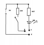
A 9 volt battery a 4K7 resistor a 22K or thereabouts and an LED is all you need to identify C B E
The LED should only light when the switch is closed and the transistor gets base current.
If the LED is lit (or even glows a little) when the switch is open the connections are wrong or the device is faulty.
As drawn and it's for NPN devices. To identify the PNP ones reverse the battery and the LED and test as before.
You know which are NPN and PNP from the device number.
Japanese transistors of that vintage were always 2SCxxxx or 2SAxxxx etc
I would start again... check the passive components (the resistors) and refit new semiconductors but make sure you know the pinouts.
A 9 volt battery a 4K7 resistor a 22K or thereabouts and an LED is all you need to identify C B E
The LED should only light when the switch is closed and the transistor gets base current.
If the LED is lit (or even glows a little) when the switch is open the connections are wrong or the device is faulty.
As drawn and it's for NPN devices. To identify the PNP ones reverse the battery and the LED and test as before.
You know which are NPN and PNP from the device number.
Attachments
Ive replaced all the non driver/output transistors with BC639 & BC640's for testing, and all is well, all crackling & popping is gone, except the amp is really quiet.. BC639's&640's feature much lower gain values, is this why?
I havent adjusted the biasing
Although when testing before changing transistors, it was just as quiet...
I havent adjusted the biasing
Although when testing before changing transistors, it was just as quiet...
Thanks, has been a great help to me.Hi here is the circuit hope it helps
regards jim
Help - I need to repair my KA-1500
Many thanks to Mooly and Big Jim for the info and useful advice posted on this thread. I was given a KA-1500 which someone else tried to repair previously. The 0.47 x2 resistor was broken (burnt?) - now replaced. I haven't switched it on yet because I am familiarising myself with the pcb and component layout.
I am confused because the circuit and pcb component value/identifier do not match! Can someone tell me what their pcb reference no. is?
Also, the wires from the phono and tuner sockets are missing and I don't know where these go on the pcb. Then there is a wire from the pcb which has been disconnected and is lying free.
Can someone provide me with a service manual for this amplifier? (I already have the circuit diagram posted here - Thanks.) I need it in order to identify which component is which (pcb to circuit diag).
Many thanks in advance.
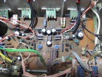
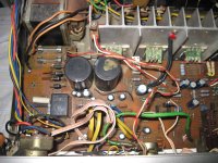
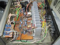
Thanks Mooly and Sakis for your input. I suspect that my amp is not the original KA-1500. The PCB is marked X09-1450-10 A/11 (Mark II ???) while the schema quotes X09-1200-21.
Moreover, I notice there are only 2 fuses on the pcb and both are 6A 250V (unlike those stated on the schema - 3A). Also on the schematic there is another fuse (Fm3) on the pcb which is not there but on the chassis (3A).
I made a resistance check of the 2 THm (thermistors? - fixed on the heatsink) and they both measure around 13K. I tried to find the 330R from the emitters of the driver trans but I couldn't find them.
On the pcb there is a black box-type component marked 24V, possibly a relay. I couldn't see this on the schematic. There are also a couple of 5-legged transistors (IC's?) which are not on the schema.
I still have to power up the unit (with bulb in series) so I am posting some photos in the hope that some member can identify with some certainty this amp's pcb.
Thanks in advance for your help
Attachments
from he way you post and describe things its rather obvious that you don't have skills enough to work farther this amp Then again the amplifier itself is in a very bad condition .
you will get some general help from this http://www.diyaudio.com/forums/solid-state/136261-vintage-amplifier-repair-upgrade-manual.html but other than that dont expect much ...
( malta is very close to greece you may as well sent it in i can have it fixed for you )
you will get some general help from this http://www.diyaudio.com/forums/solid-state/136261-vintage-amplifier-repair-upgrade-manual.html but other than that dont expect much ...
( malta is very close to greece you may as well sent it in i can have it fixed for you )
OK Sakis, your guess is correct. I don't have much servicing experience. I did build and restore a few valve amps and a couple of transistor amps with a lot of help from friends on this and other sites. That's the exciting fun of DIY getting something to work again and doing it yourself!!
Thanks for the link to your servicing manual. Very interesting but more or less I read about these restoration/modification tips. From your experience and knowledge of 70s vintage amps, can you tell what model it is? Do you have a circuit diagram for it? I admit that it is in a rather bad shape inside but that is something that can be rectified once it is working correctly.
Before sending it to Greece for servicing I'd like to try my hand at it and learn something in the process!!
sent it to Greece was more intended to be as a joke since indeed we are close and still will be an option for you
as i said previously in my library exist over 2000 schematics and of course the KA1500 but trust me exist only for reference and are actually used very rare. An amplifier of this class is a walk in the park and most of the information you need is already given in the composed service manual ...
I could provide some additional tips but the basis is there ...fault finding and trouble shooting is about procedure neither me nor anybody else in this forum will ever tell you """replace this resistor or that transistor and you are done """
I am not trying to kill your diy spirit i am just telling you simple facts .... half of the problems of this amp will be self cured when you clean everything and replace all capacitors after that we may talk again ...
Kind regards sakis
First thing I would do is give it a clean with with foam cleaner and a soft brush... pretty much everything exept the mains transformer really.
In the course of the day job I've washed dozens of TV chassis and VCR pcbs etc to clean them up. Then a good rinse under a hot tap, use paper to dry as much excess as possible and then leave to dry.
The large black box is a relay and the 5 legged things look like dual transistors. That's two identical ones (with common emitter usually) in one package to provide close thermal coupling for minimum DC drift with temperature. Could also be FET's too.
It looks to have a hard life tbh but should be fixable and is great for learning on.
Thanks Mooly for your practical tips. I cleaned the pcb and components with alcohol but somehow the dirt re-surfaces. I also cleaned the facia and it looks a 100 times better now. I also cleaned the switches and pots with WD40 (cleaner). I agree, it wasn't well cared for and whoever tried to repair it made a mess with the wiring.
From the photos I posted, does it look like a KA-1500 or a MkII? If a Mk II there are quite a few component changes from what I've seen.
And the in-circuit resistance of the thermistors at 13K, does that sound OK? The relay there, is it for speaker protection or as a slow turn-on device? It doesn't feature on the circuit diagram. It would be nice (and I suppose helpful) to have the circuit diagram as a point of reference when I switch it on (assuming the test bulb doesn't light up!)
Thanks all for your help.
I can't say what it is from the pictures tbh. It doesn't look like the one in the circuit diagram at the start of this thread. That doesn't seem to have the relay or dual input transistors.
What does the front panel show as a model number ?
If the relay contacts go to the speaker sockets then it's a speaker delay and maybe DC offset protection too.
I can't see it having a slow start.
The thermistors should be fine unless physically damaged. The resistance in circuit will be misleading and without knowing the device and having a data sheet for it it's impossible to guess what the "cold" resistance is. Sure to be alright though.
- Status
- This old topic is closed. If you want to reopen this topic, contact a moderator using the "Report Post" button.
- Home
- Amplifiers
- Solid State
- Kenwood KA-1500 transistor fault?