Pavel,
you set me on the right track. It's obviously my FG/Probes/Scope setup that limits accuracy, Both the rise time with 2Mhz and the 'blip' are there if I probe my function generator directly. (The probe was slightly miscompensated, though) Guess that are new arguments for a better (and expensive...) probe? Or new FG?
So, the buffer's rise time will be smaller and most probably there won't be any crossover distortion.
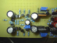
So I will try to improve stablity. Any comments to the physical implementation of the buffer? The face-to-face parts are the output stage.
(btw: how exactly is cross conduction defined? I'm mixed up sometimes, because there are some terms where I only know the german word, some others I only know in english. And many I don't at all )
)
EDIT: the 30Vpp 2Mhz square looks even better. One cannot tell, however, how much it would improve further with better measurement equipment
Rüdiger
you set me on the right track. It's obviously my FG/Probes/Scope setup that limits accuracy, Both the rise time with 2Mhz and the 'blip' are there if I probe my function generator directly. (The probe was slightly miscompensated, though) Guess that are new arguments for a better (and expensive...) probe? Or new FG?
So, the buffer's rise time will be smaller and most probably there won't be any crossover distortion.
So I will try to improve stablity. Any comments to the physical implementation of the buffer? The face-to-face parts are the output stage.
(btw: how exactly is cross conduction defined? I'm mixed up sometimes, because there are some terms where I only know the german word, some others I only know in english. And many I don't at all
)EDIT: the 30Vpp 2Mhz square looks even better. One cannot tell, however, how much it would improve further with better measurement equipment
Rüdiger
Attachments
Hi,
I hope this is correct.
Cross conduction is when both output devices carry unintended current from rail to rail.
When operating slowly, the normal bias across the output devices swings complementary fashion in the push/pull output stage.
As the current in one device swings low the current in the complementary device swings high and the difference in current flows to the output. At quiescent bias the two currents are equal and zero current flows to the load.
At high frequency the speed of the devices becomes significant.
The switching on time and the switching off time differences start to dominate the high frequency behaviour.
Usually a slow turn off time is the parameter causing cross conduction problems. Assume we start with the upper device flowing maximum operational current and the lower device at minimum current. The difference still flows to output. A short time later the drive circuit has told the top output device to start turning off (=less current) and the lower device to turn on (=more current). The top device disobeys this instruction and continues supplying current but the faster turn on time of the lower device allows it to follow the driver circuit instruction. So we have the lower device passing more current and the upper device still passing a higher current than instructed. This excess current from the upper device flows rail to rail.
As frequency is raised even higher the excess current flow from rail to rail due to slow turn off (in either device) becomes dominant and starts to raise the temperature of the devices due to excess dissipation. Continue this for too long and the output stage will overheat or in worst case senario destroy itself.
Thanks, very instructive!
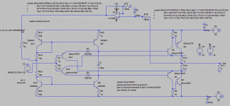
Could this cross-conduction issue be solved, at least for the sake of the output devices, with the led-clamping technique (between q1+Q2's bases in my case) as in Walt Jung's article? Or is this something else? (D3/D4 in Walt's article)
Rüdiger
Could this cross-conduction issue be solved, at least for the sake of the output devices, with the led-clamping technique (between q1+Q2's bases in my case) as in Walt Jung's article? Or is this something else? (D3/D4 in Walt's article)
Rüdiger
Hi,
again I'm no expert, but my only solution is to ensure that the adopted devices have suitable turn off/on times for the intended maximum frequency of operation and that it is better if these two times closely match each other on/off and between devices.
The time differences in effect set the limit on maximum frequency.
D3&4 are over current limiters for high output voltages into low impedance loads, just as Walt describes. This could be for hot swapping of interconnects or for a muting circuit at the input of the next stage.
AndrewT said:
D3&4 are over current limiters for high output voltages into low impedance loads, just as Walt describes. This could be for hot swapping of interconnects or for a muting circuit at the input of the next stage.
Yes, I know that's the
intention just wondering about additional effects
But I guess the diodes won't be faster than the Q's
Rüdiger
I don't think the speed of the diode is the issue.Onvinyl said:But I guess the diodes won't be faster than the Q's
They limit drive voltage to the output stage. They cannot improve the speed of turn off of the output devices, even when they are operating within the intended range of output voltages.
Cross conduction can happen when well within the intended range of voltages and load impedances. Cross conduction is an excessive frequency problem.
Find out how high your amp can go without overheating (or by measuring rail currents) and then set your input filter to remove most of this drive frequency. F-3db probably 3 or 4 octaves below the cross conduction frequency at best, maybe 5octaves below might be better/safer.
Hi, Rüdiger,
Don´t worry about cross-conduction. it is not the case. C1 help to prevent this in VERY high frequencies. for peace of mind, check if the current consumption rise with frequency.
The blip at top of senoide is only artifacts from the function generator.
the thickening in the vertical portions of square-wave is only a kind of "jitter", either by osciloscope or FG or noise.
If you have the original Tek probes, it´s OK. Only thing you need is to compensate (in X10), by using the own cal generator in the scope.
If you dont have X10 probes, go to ebay and buy some chinese 100 Mhz probes, it costs next to nothing.
Hope this help.
Marcos
thanks for the clarification.
The oscillation issue is at least partly induced through the fact, that, if the input is DC-coupled, the bias of the circuit moves with the presented input impedance widley (it doubles when driven with 50R instead of 500R, for instance).
(I have not shown pictures of the oscillating circuit so far.)
EDIT: which should not be the case, according to sim!
So, I should ensure a fixed input impedance or find a bias scheme that locks the values independently from the input situation.
And I need to check, if RC-ing on the input to limit bandwith might solve the issues. The 10pF shown yet are indeed there for stability.
thanks again,
Rüdiger
Rüdiger,
Have you thinked about add a series resistor at input?
It´s a very old trick, wich miself always used. this prevent the input transistor (and tubes, too) to turn into a common base oscillator.
About DC, it´s a diamond buffer, Ib of input transistors is cancelled.
Perhaps take care about matched beta of input transistors and/or make one of CCS adjustable, to nulling any offset. If not, when you move the potentiometer, you move the speakers, too...
Marcos
A very shy input RC (20R/10p) solved all so far detected issues.
The 20R are of course in series with the Zout of the preceding stage. With 600R, I could not see any deviation in a 20kHz square, so I'm sure that fits the bill.
I have a question, though, regarding the circuits/regulators capability of handling transients that are in the signal and then polluting the +/- voltage supply lines.
With any high frequency sine wave, I could not see any issue with the 5mV/div (the lowest I can) setitng (input with 30Vpp, and probing + or - supply line). I only get a straight line.
All the same, but with a square, I get a fast settling spike with d=40mV.
Given the ideal (=no reflections at supply lines) isn't easy to achieve, how well should these spikes be suppressed? Or isn't that an issue with audio?
Rüdiger
Power output stage?
Hi,
is it possible to build a power output stage with the topology of posting #54?.
I'm looking for an open loop (=meaning the output stage is out of the loop), Class A biased output stage in diamond topology.
An experimental amp with 15W would be fine, in the end I'm heading for min. 50W (Class A).
What I like here is the linearity of that stage, along with PSRR and voltage swing close to the rails.
Would one get it to work stable? Am I right to assume that such an output stage is relativly easy to drive?
Rüdiger
")
- Status
- This old topic is closed. If you want to reopen this topic, contact a moderator using the "Report Post" button.
- Home
- Amplifiers
- Solid State
- Jung/PMA Line-Buffer