Juma LSK as phase splitter
Prasimix,
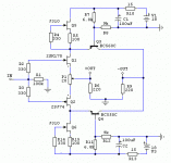
I intend to use the circuit as a phase splitter at the input to bridge tied amps. I was to use the attached schematic which Juma published on F4 thread . I did not see the CCSs in your schematic, only the simpler resistor solution there.
>Is there a chance you could still provide that option on your pcbs (J310s)? I would much appreciate it. If so, I would be interested in 4 mono (single) versions. postage to ON, Canada.
p.s. I assume there is also a neat way to jump the buffer if not needed?
Prasimix,
I intend to use the circuit as a phase splitter at the input to bridge tied amps. I was to use the attached schematic which Juma published on F4 thread . I did not see the CCSs in your schematic, only the simpler resistor solution there.
>Is there a chance you could still provide that option on your pcbs (J310s)? I would much appreciate it. If so, I would be interested in 4 mono (single) versions. postage to ON, Canada.
p.s. I assume there is also a neat way to jump the buffer if not needed?
Attachments
Yes, prasimix, that looking "more separated"! (for want of a better term!)
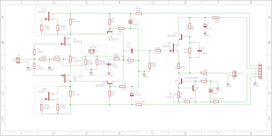
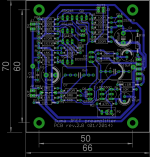
Had a bit of another look at your single gain stage version pcb again -
You know what, despite my reluctance, I'd be a bit inclined to simply run a copper link from near the centre pin of the J4 strip across the board to adjacent the R24 ground track point - could run the link underneath with an insulated sleeve, etc (replaces that long signal gnd track right around the outside)
Now, the last thing I'd like to see is the three ends of R12, R8 and R9 all together (I think R9 better going to a 'power gnd' rather than 'signal gnd', despite my earlier suggestion - sorry) to a clean GND point - let's see ..
Now that R24 is out of the way and R14 is closer to the Q4 and R9, it might be possible to move R12 directly below that same Q4 and get the neg rail to it by turning the C2 around 180* and slipping that GND track between the R13 if you lower it a bit ...
Don't know if you can tie the ends together to R8, R9 and a clean GND point - I've suddenly lost the plot a bit here, but it does seem 'do-able'! Again, not sure if it will make any difference at all, but I 'have a feeling' (!) that it will!
Oh, can move that R24 down below the C11 and move the C2 up a bit to make room (or move J2 and R18 down a bit) - while you're in that area, you can move the R14 towards the centre of the board above C7 and move C11 to be horizontal - gets a bit more room to play with a reduces stray currents around this area a bit, IMO.
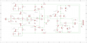
Now, the power supply brd.
Don't worry about including the thermistor and diodes in the pcb as it's simple to add them near the chassis GND terminal - this is where I do it with mine, along with the simple dc trap, etc.
If you look at the area around the J8 terminal, this is the area where the diode and transformer 'noise' is at worst (where current spikes at max) and you want to keep these as 'localised' as possible hence no big fat track between this point and the circuit central ground point - it looks a bit strange but it does make quite a difference.
This is why the main ground point is located near the caps C16, C23 - a further refinement is that the currents thru the 24 volt rails aren't the same as the higher voltage rails so theoretically should have separate grounding tracks but at the same time, should mate up the + and - caps ground tracks - I don't think it'll make much difference here but I'm pretty sure AndrewT would explain it a lot better.
There IS one thing that I would make some room for near that J8 terminal and that's a R - C snubber across the secondary windings - there's been plenty of discussions over the years about the relative merits of this simple device but it seems to have fallen from use these last few years - if it's 'done right', it can make an enormous difference to the whole sound of the circuit it's powering (there's a recent kit offer about that Quazimodo test ringer circuit that makes it very simple to find the correct resistor for the job - highly recommended)
Hope this is of some use - again, much of this is just my opinion and there are other ways of doing things ....
Had a bit of another look at your single gain stage version pcb again -
You know what, despite my reluctance, I'd be a bit inclined to simply run a copper link from near the centre pin of the J4 strip across the board to adjacent the R24 ground track point - could run the link underneath with an insulated sleeve, etc (replaces that long signal gnd track right around the outside)
Now, the last thing I'd like to see is the three ends of R12, R8 and R9 all together (I think R9 better going to a 'power gnd' rather than 'signal gnd', despite my earlier suggestion - sorry) to a clean GND point - let's see ..
Now that R24 is out of the way and R14 is closer to the Q4 and R9, it might be possible to move R12 directly below that same Q4 and get the neg rail to it by turning the C2 around 180* and slipping that GND track between the R13 if you lower it a bit ...
Don't know if you can tie the ends together to R8, R9 and a clean GND point - I've suddenly lost the plot a bit here, but it does seem 'do-able'! Again, not sure if it will make any difference at all, but I 'have a feeling' (!) that it will!
Oh, can move that R24 down below the C11 and move the C2 up a bit to make room (or move J2 and R18 down a bit) - while you're in that area, you can move the R14 towards the centre of the board above C7 and move C11 to be horizontal - gets a bit more room to play with a reduces stray currents around this area a bit, IMO.
Now, the power supply brd.
Don't worry about including the thermistor and diodes in the pcb as it's simple to add them near the chassis GND terminal - this is where I do it with mine, along with the simple dc trap, etc.
If you look at the area around the J8 terminal, this is the area where the diode and transformer 'noise' is at worst (where current spikes at max) and you want to keep these as 'localised' as possible hence no big fat track between this point and the circuit central ground point - it looks a bit strange but it does make quite a difference.
This is why the main ground point is located near the caps C16, C23 - a further refinement is that the currents thru the 24 volt rails aren't the same as the higher voltage rails so theoretically should have separate grounding tracks but at the same time, should mate up the + and - caps ground tracks - I don't think it'll make much difference here but I'm pretty sure AndrewT would explain it a lot better.
There IS one thing that I would make some room for near that J8 terminal and that's a R - C snubber across the secondary windings - there's been plenty of discussions over the years about the relative merits of this simple device but it seems to have fallen from use these last few years - if it's 'done right', it can make an enormous difference to the whole sound of the circuit it's powering (there's a recent kit offer about that Quazimodo test ringer circuit that makes it very simple to find the correct resistor for the job - highly recommended)
Hope this is of some use - again, much of this is just my opinion and there are other ways of doing things ....
Juma posted a video with Nelson explaining the curcuit
I think Nelson is saying jfet availability will be no problem
not sure what is said exactly
but watch it anyway, it is quite good
Hi
Can you post a link to the vid please?
1. post in Jumas's thread
Okay, I was looking at the more recent posts. I will have a look. Thanks
Prasimix,
I intend to use the circuit as a phase splitter at the input to bridge tied amps. I was to use the attached schematic which Juma published on F4 thread . I did not see the CCSs in your schematic, only the simpler resistor solution there.
>Is there a chance you could still provide that option on your pcbs (J310s)? I would much appreciate it. If so, I would be interested in 4 mono (single) versions. postage to ON, Canada.
p.s. I assume there is also a neat way to jump the buffer if not needed?
Hi koja, do you think that additional fets should be mandatory or just optional if someone wants to use it as phase splitter?
There IS one thing that I would make some room for near that J8 terminal and that's a R - C snubber across the secondary windings - there's been plenty of discussions over the years about the relative merits of this simple device but it seems to have fallen from use these last few years - if it's 'done right', it can make an enormous difference to the whole sound of the circuit it's powering (there's a recent kit offer about that Quazimodo test ringer circuit that makes it very simple to find the correct resistor for the job - highly recommended)
What should I do here? Just try to find some room for RC?
CCS transistors
Prasimix, those are not limited to phase splitter use. everybody would benefit from them. this is if one does not mind matching the CCS transistors (they need to be matched). if someone does find that inconvenient, they can always opt to leave them out and go with a simple resistor.
pozdrav,
Koja
Prasimix, those are not limited to phase splitter use. everybody would benefit from them. this is if one does not mind matching the CCS transistors (they need to be matched). if someone does find that inconvenient, they can always opt to leave them out and go with a simple resistor.
pozdrav,
Koja
prasimix:
I cannot edit your spreadsheet for some odd reason. Please put me down for 4 single preamp channels and 4 single power supply channels. Shipping will be to the US. It's possible I may want to increase the order and will know in the next few days.
Regards,
Scott
Thanks Scott, I added you into list. Possibly you need to be registered on ZOHO for making changes in the sheet. Who knows.
Yes, prasimix, that looking "more separated"! (for want of a better term!)
Had a bit of another look at your single gain stage version pcb again -
You know what, despite my reluctance, I'd be a bit inclined to simply run a copper link from near the centre pin of the J4 strip across the board to adjacent the R24 ground track point - could run the link underneath with an insulated sleeve, etc (replaces that long signal gnd track right around the outside)
Now, the last thing I'd like to see is the three ends of R12, R8 and R9 all together (I think R9 better going to a 'power gnd' rather than 'signal gnd', despite my earlier suggestion - sorry) to a clean GND point - let's see ..
Now that R24 is out of the way and R14 is closer to the Q4 and R9, it might be possible to move R12 directly below that same Q4 and get the neg rail to it by turning the C2 around 180* and slipping that GND track between the R13 if you lower it a bit ...
Don't know if you can tie the ends together to R8, R9 and a clean GND point - I've suddenly lost the plot a bit here, but it does seem 'do-able'! Again, not sure if it will make any difference at all, but I 'have a feeling' (!) that it will!
Oh, can move that R24 down below the C11 and move the C2 up a bit to make room (or move J2 and R18 down a bit) - while you're in that area, you can move the R14 towards the centre of the board above C7 and move C11 to be horizontal - gets a bit more room to play with a reduces stray currents around this area a bit, IMO.
jameshillj, I move R9 down close to out connector and connect it instead of power gnd to signal gnd where I think it belongs. If that is wrong we can simply connect it again to power gnd. R24 is also now closer to out connector.
Prasimix,
I intend to use the circuit as a phase splitter at the input to bridge tied amps. I was to use the attached schematic which Juma published on F4 thread . I did not see the CCSs in your schematic, only the simpler resistor solution there.
>Is there a chance you could still provide that option on your pcbs (J310s)? I would much appreciate it. If so, I would be interested in 4 mono (single) versions. postage to ON, Canada.
p.s. I assume there is also a neat way to jump the buffer if not needed?
Koja, please check schematic. I marked CCS and output section which is terminated on OUT2 connector. Personally I don't like its place on PCB but that's only what I find that is close to board edge. Maybe there is another possibility to put it somewhere above Q7 in the middle of the PCB. If someone wants to "jump the buffer" he need to put jumper on R9A position and use OUT2 connector. Another possibility is to introduce place for the jumper to use OUT connector.
If new changes is ok, I can try to add it in dual channel layout together with jameshillj suggestion for moving main gnd point.
Attachments
I like simple circuits and as it seems that the LSKpre will work just fine with the F5 without buffer, I will go this route. The more simple this "buffer bypass" can be done, the better (for me)If someone wants to "jump the buffer" he need to put jumper on R9A position and use OUT2 connector. Another possibility is to introduce place for the jumper to use OUT connector.
")
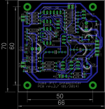
It's getting quite crowded in there Prasimix!
I hope you don't mind my 'spouting off' about your pcb design - rev.2.6 and rev.2.7 are coming along nicely, IMO.
If you don't mind a bit more 'nit-picking' ....
I would shift R6 back over to it's old position below R1 and just use the extra length of the resistor lead to jump across to the pot P1 mid pin - maybe a bit of sleeve, and simple!
I do like the new position of R9 - you could maybe move it up between R12 and R14 to gain a bit of room and reduce tracking - not much in it tho.
If you move R22 to the right and connect it to the -24 volt pin of J4 outside of the -33v track, this allows you to straighten the track to C4 and you could move R17 up below R22 - this gives a bit more room to shift R21 to the right and makes the tracks to P2a bit simpler - will need to move those transistor down a bit and this also allows room to move R19 above Q5.
That's about it - perhaps you might add a single donut near the 0volt pin of the J4 and another one near the grd track adjacent C11 for me, if you would (for a direct copper link across the board!) ....
The caps C6 and C7 are about 9 x 18mm, yes? What type of caps did you have in mind for these?
Don't worry about the snubber on the power supply -board - there's only a few that will want to try it, and can just add the components across the transformer terminals, as per usual
However, with the floating ground network of the thermistors and diodes, hmm, that would be quite neat to include it if there's room somewhere - not essential tho ....
I like simple circuits and as it seems that the LSKpre will work just fine with the F5 without buffer, I will go this route. The more simple this "buffer bypass" can be done, the better (for me)
Added room for JP1 close to OUT connector.
It's getting quite crowded in there Prasimix!
I hope you don't mind my 'spouting off' about your pcb design - rev.2.6 and rev.2.7 are coming along nicely, IMO.
If you don't mind a bit more 'nit-picking' ....
Not at all! Please just continue with your effort. I'd like at the end to have better solution and your and other members suggestions is more then welcome.
I think that we have now almost everything on right place.I would shift R6 back over to it's old position below R1 and just use the extra length of the resistor lead to jump across to the pot P1 mid pin - maybe a bit of sleeve, and simple!
I do like the new position of R9 - you could maybe move it up between R12 and R14 to gain a bit of room and reduce tracking - not much in it tho.
If you move R22 to the right and connect it to the -24 volt pin of J4 outside of the -33v track, this allows you to straighten the track to C4 and you could move R17 up below R22 - this gives a bit more room to shift R21 to the right and makes the tracks to P2a bit simpler - will need to move those transistor down a bit and this also allows room to move R19 above Q5.
That's about it - perhaps you might add a single donut near the 0volt pin of the J4 and another one near the grd track adjacent C11 for me, if you would (for a direct copper link across the board!) ....
Please check attached BOM. I found one 10uF small enough.The caps C6 and C7 are about 9 x 18mm, yes? What type of caps did you have in mind for these?
Don't worry about the snubber on the power supply -board - there's only a few that will want to try it, and can just add the components across the transformer terminals, as per usual
However, with the floating ground network of the thermistors and diodes, hmm, that would be quite neat to include it if there's room somewhere - not essential tho ....
If that is more or less everything for single channel layout, I can try to do the same on the dual channel and also publish latest revision of PS.
Attachments
Wich resistor brand
at Farnell is it wise to chose?
There are MANY to choose from..
This and some other technical questions asked before maybe should be posted on main thread to make Juma and other members who is more experienced aware of them?
Is the price for the stereo verision 5 EURO?
In that case I´ll take 1 more..
Edit:I am from Sweden.
No, single channel PCB is 5EUR, therefore for stereo you need to spent 10EUR
Edit: Sorry, I put by mistake that price for dual channel. It's now corrected in GB list.
Last edited:
- Status
- This old topic is closed. If you want to reopen this topic, contact a moderator using the "Report Post" button.
- Home
- Group Buys
- Juma's LSK Preamp - through hole version