Hi
Can somebody points out where can I get the Gerbers files?
Thanks
Fab
Hello Fab,
Post 280 gives the gerbers.
I have it shared also on pcbway where you could order the PCBs OR download the gerbers along with sch , stuffing guide, link to mouser BoM example (made for DIYA user Juntuin for 24V output), etc.
Here is the link.
W61084ASN2_juma cap multi-R4 EXT DIODES+led+gnd- Share Project - PCBWay
Regarding board house preference, I now prefer pcbway. They are top notch, with excellent customer support.
EasyEDA now no longer supports manufacturing and direct you to JLC pcb. For one of my orders (DLH amp), the silk was not properly printed by JLCpcb.
Regards
Prasi
Last edited:
Prasi - Thanks for the help. I tried Eagle, but got frustrated with it quickly. I imagine I'll learn eventually.
@Skylar88 - I tried KiCad, and with a little struggle ended up with a reasonable looking board.
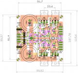
My attempt at the CapMult is nowhere as compact as some here, but it's a single supply solution that fits 2 per 100mm sq boards.
- It has 1.5mm traces for the rails (and kept as short as I could manage).
- The traces for the 4700 are 1mm and the rest are 0.25mm. I have no idea if any of them are sufficient or not.
- The plan was to have bare copper on the bottom, silk screen on the top, and reinforce the power traces by soldering a bit of wire on top of the trace to increase the cross-sectional area (and therefore the power handling).
- I tried to leave a fair bit of space around the MOSFET so it could get a reasonable heat sink on it.
- the holes are just under 40mm across and just under 90mm on the long axis, so they should bolt into the standard 1cm grid.
- the big cap is way bigger than necessary, it has a 30mm diameter footprint, but better safe than sorry. I didn't check to see if the 30mm caps had larger lead spacing... I'll have to look into that.
- Any thoughts on the part layout or trace sizes/widths?
- I also could use some help figuring out how to officially mark the edge of the board (you can see that it's just in the silkscreen).
- Also, did I define the holes correctly?
- What other things can you spot that might need to be fixed before taking the plunge and getting some made?
kking85743,
WHy dont you try sprint, its very easy and within an hour you will be able to make a workable layout.
Regarding your current PCB, please find my below initial comments.
1. Its better to keep together input and its gnd. similarly output and its ground.
2. make traces as thick as possible.
3. You need a proper heatsink for the mosfet, so think and position you mosfet accordingly.
4. keep the components connected to gate as close as possible to gate.
long way to go. but you will eventually get there. Keep it up!.
regards
Prasi
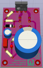
The 5W resistors are across the big 47mF caps are the capacitor discharge device and diode damping load, yes?
The photo shows "MILLS 30" on the lower resistor - perhaps they aren't actually 3kR but maybe 30R and that would sink about 13W
Hi Jameshillj,
You were exactly right!! But even worse, they were 3R!! When I remove them from the board and measured them, they were toasted.
I got into trouble because I ‘assumed’ the label on the bag that said 3K was correct. And we all know what happens when you ‘assume’

Totally my mistake, I should have measured them. I didn’t have any 3K resistors on hand, so I put two 1.5K resistors in series underneath the board.
The Juma E-P capMx works as it should now
kking85743,
WHy dont you try sprint, its very easy and within an hour you will be able to make a workable layout.
Regarding your current PCB, please find my below initial comments.
1. Its better to keep together input and its gnd. similarly output and its ground.
2. make traces as thick as possible.
3. You need a proper heatsink for the mosfet, so think and position you mosfet accordingly.
4. keep the components connected to gate as close as possible to gate.
long way to go. but you will eventually get there. Keep it up!.
regards
Prasi
Thanks for the input.
Questions arising from your responses:
(1) For small signal, keeping signal and ground close is critical. This is for a 24v power supply, and at 1.5-1.7A, I considered the shortest path for the high-current flow to be a more critical issue. Any thoughts on this trade-off?
(2a) "...as thick as possible." True, I keep forgetting circuit boards are a subtractive process. Will 1mm be a reasonable size for nominal traces? Should my 1.5mm power traces be even larger? Your ground bus up the middle of your dual polarity power supply board does look quite impressive in its width.
(2b) On a related note, at 1.5-1.7A, how wide should a trace be? I know it depends on how thick the copper is, but I don't have any idea how to find out (or specify) this parameter. I considered keeping screening off those traces and laying a wire over it and soldering it down, to increase the cross-sectional area of the trace or soldering on a wire across the bottom from point-to-point to share the current load. Or am I killing it to death? 8)
(3) I thought I left a reasonable amount of space around the MOSFET. How much more would you have left? I presume I'll be using a fairly simple (if heavily finned) heat sink (see note below). I have 15mm of space between the front of the MOSFET and the big cap (I drew a 30mm part to make sure there was some room, but am using a 20mm part, the smaller circle), and "infinite" space on the side where the sink actually bolts (presuming the spade and screw at the top of the board prove to be no issue).
(4) How close is too close? By my measurement, from the input there is 15mm of copper to the diode, and an extra 7.5 to the resistor. On the other side of the pair is 7.5 from resistor to diode, and another 7.5 to the gate resistor, followed by 10mm to the gate. Since the diode is an escape valve for the cap, the actual signal path is 2 resistor lengths plus 47.5mm of copper. Does that really make a noticeable difference? Redesign options include swapping diode and resistor (15mm shorter path), sliding that pair closer to the input, and rotating the gate resistor to horizontal and moving it to be just below the gate, shortening both the R-G copper trace and the R-R copper trace. Overkill?
Additional questions:
- One of my earlier questions was about how big a heat sink was needed, and I never really got a particularly useful answer... I'm using the following figures as my starting point - 8W to dissipate, T.max 60C, T.amb 35C (inside the amp case); so 25C rise for 8W and a TO-247 case. Based on that info, it appears that this ( https://www.digikey.com/product-detail/en/ohmite/RA-T2X-51E/RA-T2X-51E-ND/2416489 ) is sufficient, as it says it will go up 20C while dissipating 8W at a claimed Tr of 3.5C/W, with others showing greater efficiency. It is only about 25mm thick, presuming half/half split, it comes 12.5mm towards cap from back of device, so (allowing for thickness of part) comes about halfway to the big cap (7.5mm away). That gap can be made larger by leaning the device away from the cap.
- Plan B for the heat sink is to move the MOSFET to the top edge of the board and bolt it the base-plate of the amp and hope that the airflow up from the slots of the bottom cover is sufficient to keep things cool. I'm using a 2U Dissipante case with baseplate.
- How much tighter would you pack the parts? I have about 7.5mm between most pads at closest. I've seen some packed in at 5mm between, but how close is too close? I'm as much concerned with solderability as with proximity issues (thermal, overall packing of stuff, etc...)
Any additional thoughts or ideas based on these additional questions?
Hi PrasiHello Fab,
Post 280 gives the gerbers.
I have it shared also on pcbway where you could order the PCBs OR download the gerbers along with sch , stuffing guide, link to mouser BoM example (made for DIYA user Juntuin for 24V output), etc.
Here is the link.
W61084ASN2_juma cap multi-R4 EXT DIODES+led+gnd- Share Project - PCBWay
Regarding board house preference, I now prefer pcbway. They are top notch, with excellent customer support.
EasyEDA now no longer supports manufacturing and direct you to JLC pcb. For one of my orders (DLH amp), the silk was not properly printed by JLCpcb.
Regards
Prasi
Thanks fo the info and for sharing
Aside the fact that the pcb size could be bigger, any reason to not include fast transient soft recovery diodes as rectifier - which should have been great, at least for me....
Fab
I would go along with whatever you wish.
Steve.
Since it is for high current power supply I will go for 2oz copper , 2mm thick and gold immersion. Black color also because peoples like that from feed-back I have already received for other pcbs...
Anyway, the big cost drivers are the shipment and duty taxes for small quantity ordering...
Fab
Hi Prasi
Thanks fo the info and for sharing
Aside the fact that the pcb size could be bigger, any reason to not include fast transient soft recovery diodes as rectifier - which should have been great, at least for me....
Fab
There’s a version with that feature posted earlier by Prasi as well. It was I who asked him to make it with external block bridges.
Thanks for the input.
Questions arising from your responses:
(1) For small signal, keeping signal and ground close is critical. This is for a 24v power supply, and at 1.5-1.7A, I considered the shortest path for the high-current flow to be a more critical issue. Any thoughts on this trade-off?
(2a) "...as thick as possible." True, I keep forgetting circuit boards are a subtractive process. Will 1mm be a reasonable size for nominal traces? Should my 1.5mm power traces be even larger? Your ground bus up the middle of your dual polarity power supply board does look quite impressive in its width.
(2b) On a related note, at 1.5-1.7A, how wide should a trace be? I know it depends on how thick the copper is, but I don't have any idea how to find out (or specify) this parameter. I considered keeping screening off those traces and laying a wire over it and soldering it down, to increase the cross-sectional area of the trace or soldering on a wire across the bottom from point-to-point to share the current load. Or am I killing it to death? 8)
(3) I thought I left a reasonable amount of space around the MOSFET. How much more would you have left? I presume I'll be using a fairly simple (if heavily finned) heat sink (see note below). I have 15mm of space between the front of the MOSFET and the big cap (I drew a 30mm part to make sure there was some room, but am using a 20mm part, the smaller circle), and "infinite" space on the side where the sink actually bolts (presuming the spade and screw at the top of the board prove to be no issue).
(4) How close is too close? By my measurement, from the input there is 15mm of copper to the diode, and an extra 7.5 to the resistor. On the other side of the pair is 7.5 from resistor to diode, and another 7.5 to the gate resistor, followed by 10mm to the gate. Since the diode is an escape valve for the cap, the actual signal path is 2 resistor lengths plus 47.5mm of copper. Does that really make a noticeable difference? Redesign options include swapping diode and resistor (15mm shorter path), sliding that pair closer to the input, and rotating the gate resistor to horizontal and moving it to be just below the gate, shortening both the R-G copper trace and the R-R copper trace. Overkill?
Additional questions:
- One of my earlier questions was about how big a heat sink was needed, and I never really got a particularly useful answer... I'm using the following figures as my starting point - 8W to dissipate, T.max 60C, T.amb 35C (inside the amp case); so 25C rise for 8W and a TO-247 case. Based on that info, it appears that this ( https://www.digikey.com/product-detail/en/ohmite/RA-T2X-51E/RA-T2X-51E-ND/2416489 ) is sufficient, as it says it will go up 20C while dissipating 8W at a claimed Tr of 3.5C/W, with others showing greater efficiency. It is only about 25mm thick, presuming half/half split, it comes 12.5mm towards cap from back of device, so (allowing for thickness of part) comes about halfway to the big cap (7.5mm away). That gap can be made larger by leaning the device away from the cap.
- Plan B for the heat sink is to move the MOSFET to the top edge of the board and bolt it the base-plate of the amp and hope that the airflow up from the slots of the bottom cover is sufficient to keep things cool. I'm using a 2U Dissipante case with baseplate.
- How much tighter would you pack the parts? I have about 7.5mm between most pads at closest. I've seen some packed in at 5mm between, but how close is too close? I'm as much concerned with solderability as with proximity issues (thermal, overall packing of stuff, etc...)
Any additional thoughts or ideas based on these additional questions?
---
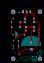
latest updates to the board:
(1) power in/out as close as possible.
(2) all traces are 2mm, except power to/from MOSFET, which are 3.3 and the buss between ground lugs, at 4mm. How thick should they be? How does one specify thickness of copper?
(3) with the MOSFET on the end, it can be bolted to the chassis or left standing with tons of space for any heat sink.
(4) Things are now closer, how much more should I squish things, or is that good enough for now?
Any other thoughts on cooling for the MOSFET?
Attachments
Hi Jameshillj,
You were exactly right!! But even worse, they were 3R!! When I remove them from the board and measured them, they were toasted.
I got into trouble because I ‘assumed’ the label on the bag that said 3K was correct. And we all know what happens when you ‘assume’
Totally my mistake, I should have measured them. I didn’t have any 3K resistors on hand, so I put two 1.5K resistors in series underneath the board.
The Juma E-P capMx works as it should now
Hi Vunce,
Glad you could sort the issue.
you made the poor little resistor dissipate almost 250w
. RIP.Did you find out about the transformer. Are you able to solve it?
Regards
Prasi
Hi Vunce,
Glad you could sort the issue.
you made the poor little resistor dissipate almost 250w
Did you find out about the transformer. Are you able to solve it?
Regards
Prasi
Hi Prasi,
Those little guys burnt good
The transformer secondaries measure 20.3vac without load, I don’t think that’s the problem. My next move is to remove the capMx board and replace with a standard CRC type and see if the dc voltage increases more than the 4.5vdc drop from the capMx.
Regards
kking85743,
WHy dont you try sprint, its very easy and within an hour you will be able to make a workable layout.
Regarding your current PCB, please find my below initial comments.
1. Its better to keep together input and its gnd. similarly output and its ground.
2. make traces as thick as possible.
3. You need a proper heatsink for the mosfet, so think and position you mosfet accordingly.
4. keep the components connected to gate as close as possible to gate.
long way to go. but you will eventually get there. Keep it up!.
regards
Prasi
Greetings Prasi (and anyone else who wants to chime in):
After the latest updates to the board (using KiCad), here are my responses to your initial comments (above), along with some additional questions: (Images of the latest board spin are available on post 430)
(1) power in/out as close as possible. Do they look close enough (10-15mm)? However it makes some other traces a bit longer (specifically the output capacitor). What do you think of the tradeoff between proximity of the power leads compared to the length for some of the other traces?
(2) all traces are 2mm wide, except power to/from MOSFET, which are 3.3 and the buss between ground lugs, at 4mm. How thick should they be? See the info (below) on the current vs temp increase for the different widths. How much heat gain on a trace is "reasonable"?
(3) with the MOSFET moved to the end of the board, it can be bolted to the chassis/heatsink or left standing with tons of space for any heat sink. The mounting should work with the 1cm "standard" grid. See additional thoughts/questions on the thermal aspect of the MOSFET below.
(4) The path to the gate is now shorter. How much more should I squish things, or is that good enough for now? The present path is: power input to resistor, to resistor, to MOSFET pin, for a total distance on board of about 20mm of copper traces and two resistor lengths.
On cooling the MOSFET:
~~~~~~~~~~~~~~~~~~~~~~
One of my earlier questions was about how big a heat sink was needed, and I never really got a particularly useful answer...
- I'm using the following figures as my starting point - 8W to dissipate, T.max 70C, T.amb 35C (inside the amp case); so 35C rise for 8W and a TO-247 case.
- Based on that info, it appears that this ( https://www.digikey.com/product-detail/en/ohmite/RA-T2X-51E/RA-T2X-51E-ND/2416489 ) should be close, as it says it will go up 40C while dissipating 8W at a claimed Tr of 3.5C/W. There were also other heat sinks available showing greater efficiency.
- Plan B for the heat sink: lay the MOSFET down and bolt it the base-plate of the amp (or to a heat sink, although the space inside my case doesn't support this). In my case, that is to a galvanized steel baseplate and relying on the airflow up from the slots of the bottom cover to be sufficient to keep things cool. I'm using a 2U Dissipante case.
- Any other thoughts on cooling for the MOSFET?
On trace sizes:
~~~~~~~~~~~~~~~
From: The CircuitCalculator.com Blog >> PCB Trace Width Calculator (see the web page Comments section for a discussion of the limitations of the calculations due to limits in the paper on which they are based)
Legend:
- Current is in amps, flowing on the trace
- Temp Rise is in degrees C, how much warmer the trace will become at that current
- Width is trace width in mm (on my board, power is 3.3mm and the rest are 2mm)
- 1 oz Copper is the default
MOSFET to/from power connectors
Current Temp Rise Width Temp Rise at same Current for 4mm trace (ground buss)
2.8 2 3.30 1.46
4.2 5 3.31 3.6
5.7 10 3.31 7.3
(still having trouble with tables - in short 5.7A on an inch long 3.3mm trace at 1 oz thickness results in a 10 degree rise in temp, 4.2 amps results in a 5C rise, 2.8A gives a 2C rise, so the expected 1.5-1.7A should be trivial)
output capacitor to/from power connectors
Current Temp Rise Width
1.95 2 2
2.9 5 1.99
4 10 2
(still having trouble with tables - in short 4A on a 2 inch long 2mm trace at 1 oz thickness results in a 10 degree rise in temp, 2.9 amps results in a 5C rise - no idea what current might flow here - probably only short bursts to support sudden volume increase or hard-hitting bass)
The page indicates that a 10C rise is considered quite reasonable, but I was wondering what others think. The calculations are extrapolated below 10C, as that was the baseline for the data retrieved in the paper cited as the source for the calculations.
Any thoughts on peak/surge currents? My simulations didn't show much change in currents even with on/off switches, so I'm not anticipating much, but don't know what I don't know... Note this is for supplying power to an ACA, so it's a Class A, with limited current swings.
Final thoughts on shape/size:
~~~~~~~~~~~~~~~~~~~
The overall shape of the board matches my needs, as I have long thin spaces on the baseplate available for the boards (one per channel) and was trying to stay under 100mm for two boards. I am thinking about trying an additional layout that might be able to mount on a 2U heatsink. I'll post here if I decide to give it a shot.
Last edited:
Hello king,
Why all that copper needs to etched away? If you retain more of it, the less etchant it needs. What I learnt here through distinguished members, is its just not the current capability of trace, but also inductance.
regarding cooling and heatsinking, see jameshillj post, allow for 25 deg rise over ambient with ~8W dissipation.
Also , in most cases, the chassis space is at a premium with lot of different modules and PCBs, so I try to keep my designs compact and which is also cheaper to manufacture.
All the best.
regards
Prasi
Last edited:
Ir's a bit more than that actually - 1.7A x 4.5v = 7.7W for each Q - there are 4 of them, so heat = approx 30w and if allowable temp rise about 25*C, the heatsink needs to be about 0.8*C/W in open air - so this will require a well-vented chassis or add a small fan
Perhaps it might be worth looking at another design of the pcb so the CMx transistor pairs could be mounted to each channel's main heatsinks next to the amp boards - not the simplest method, and adds more components. but it's one way to get around the 'excess heat problem' - the small Kuartlotron boards are quite easy to do this, for example, but they're only the final part of the supply
Or use transistors with lower voltage drop - we're not tied exclusively to the IRFPs
I mounted the heatsink with Prasi's completed board (with the same IRFPs) over the bottom panel vents but had to increase the heatsink size to about the 0.8*C/W size (just fitted it in!) and it has a temp rise about the 25*C with the well perforated top panel plus a 10mm gap next to the internal side of the heatsinks on the bottom panel for extra internal airflow (added cross bars to stiffen base panel - power transformer is now bolted to front plate) - it works quite well.
Greetings:
I'm having trouble with the math. For each device (I will have a total of two boards (L/R), one near either side of the case, each with one device), dropping 8W each with a target temperature raise of 25C, that should be 3.125 C/W, right? Did you use a 0.8 W/C for overkill? How did you get to that number (even 30/25 is 1.166 C/W)? I know we need a 'fudge factor' for thermal resistance between the device and the sink, but wasn't sure how much to try to allow. In catalogs, I'm seeing perhaps (if you believe specs) 2.6 as the lowest, and many only list numbers with fans attached.
In looking at the part I'm planning on using ( infineon.com irfp250n.pdf ), the significant figures appear to be 9 & 4. If I'm understanding things right, Figure 9 tells us that we can pass 1.5A well above a case temp of 150C, Figure 4 tells us that as we go from Tj of 60C to 120C Rds climbs from a normalized value (1.0 at 25C) of roughly 1.4 at 60C to 2.2 at 120C, and at 150C climbs to 2.6 (at Vgs=10v and Id=30A, both well above what we'll be doing). It looks to be a sturdy creature - any recommendations for a stable and safe max running temperature?
Given a heat sink with something around 3.0C/W, and allowing an extra 0.5 for the pad, at 8W, we get a gain of 28C over ambient, which makes actual junction temp somewhere near 60C (interior of the box estimated at 32C, as measured at top-of-case temp). Similar info on some spec sheets show numbers ranging from 40C rise for 10W, to 25C for 6W, so I think I'm in the general range. However there seems to be a gap between device mounted sinks and 3x5" fin blocks.
As I see it, my options are as follows:
1) attach a free-standing single device heat sink (digikey 6400BG-ND, HS380-ND, CR201-75VE-ND, FA-T220-64E-ND, RA-T2X-51E-ND, or similar) with 2.6-3.5 W/C and risk it.
2) bolt it to the the galvanized steel perforated base-plate as my heat sink and hope for the best.
3) just skip it, as all I'll do is let the magic smoke out, and risk the amp.
Any thoughts or clarifying comments?
Sorry, maybe we're talking about something different here - I was writing about the power consumption of the dual CMx of Pasi's when mounted on a heatsink in the middle of the bottom of the amp's case - the arithmetic goes something like this, if I've got it right -
Each of the 4 IRFP devices has about a 4.5+ volt drop across it, yes? And if it is passing 1.7A then each device is consuming theoretically, 7.65 VA, or a round figure of say, 8 watts - there are 4 of them all busy working away (dc condition, yes?) so thus sums to 32 watts total, yes?
To restrict the temp rise of the heatsink to a 25*C rise, the heatsink rating is simple 25*C/32watts = approx 0.8*C/W - not a small piece of metal at all, but maybe the bottom plate of the amp case will be enough to accept a continuous heating of 32 watts without any problems - I don't know, and I'm not satisfied of this as a well-engineered solution, but that's just me - whatever works for you is okay.
As for working out the max junction temp and the thermal resistance of a Sil pad, etc, I generally just allow a bigger margin to try to keep the device junction temp well below 100*C as a worse case on a really hot day - a stable heatsink temp of below 50*C will be usually okay to maintain a device junction temp of about 80*C or thereabouts - I generally use 'mica & goop' heat transfer for mounting the devices - I generally use the same method/arithmetic for amplifier power transistors and try to keep the rectifier diodes even cooler than this - this isn't the only way of doing things, just my way of being a bit conservative, I guess.
I'm not too sure about some of your options - there's a number of different ways of doing this device cooling and I'd suggest exploring other ways too - remember, these CMx devices are slaving away all the time, no time off, no rest, so the heat they generate is constant
I hope this is useful info, (and correct!)
35W is about how much heat an ACA puts out - so keep that as perspective for size. However note that IRFP MOSFETs are designed to run continuously for 20yrs if cooled properly so there is no issue of them always being on, same for the actual outputs on the amp, proper. Just keep the silicon die below the recommended temps, which probably is quite a bit hotter than the usual 55C requirement which is more to make sure we don’t burn ourselves where touching the case of the amp.
Sorry, maybe we're talking about something different here - I was writing about the power consumption of the dual CMx of Pasi's when mounted on a heatsink in the middle of the bottom of the amp's case - the arithmetic goes something like this, if I've got it right -
Each of the 4 IRFP devices has about a 4.5+ volt drop across it, yes? And if it is passing 1.7A then each device is consuming theoretically, 7.65 VA, or a round figure of say, 8 watts - there are 4 of them all busy working away (dc condition, yes?) so thus sums to 32 watts total, yes?
To restrict the temp rise of the heatsink to a 25*C rise, the heatsink rating is simple 25*C/32watts = approx 0.8*C/W - not a small piece of metal at all, but maybe the bottom plate of the amp case will be enough to accept a continuous heating of 32 watts without any problems - I don't know, and I'm not satisfied of this as a well-engineered solution, but that's just me - whatever works for you is okay.
As for working out the max junction temp and the thermal resistance of a Sil pad, etc, I generally just allow a bigger margin to try to keep the device junction temp well below 100*C as a worse case on a really hot day - a stable heatsink temp of below 50*C will be usually okay to maintain a device junction temp of about 80*C or thereabouts - I generally use 'mica & goop' heat transfer for mounting the devices - I generally use the same method/arithmetic for amplifier power transistors and try to keep the rectifier diodes even cooler than this - this isn't the only way of doing things, just my way of being a bit conservative, I guess.
I'm not too sure about some of your options - there's a number of different ways of doing this device cooling and I'd suggest exploring other ways too - remember, these CMx devices are slaving away all the time, no time off, no rest, so the heat they generate is constant
I hope this is useful info, (and correct!)
Ok, now it makes more sense. Among other things I had some of my numbers upside-down when analyzing your earlier calculation for the heat sink. My application runs the same current, but I only have 2 (single sided power supply for ACA, so one circuit (and one device) for each channel). My amp layout has some space on each side, so I'm doing a single device on each board, one for the left channel, one for the right. This means each device has it's own heat sink. If I'm following the pattern correctly, that's 25C/8W, or 3.125 C/W, like I thought. I'm looking at a sink that claims to be able to drop 8W with a 40C rise, so each device will be running 65C. A little warmer than the usual target, but not unmanageable, I think.
Thanks for taking the time to help me better understand what is going on.
Same for you, X (and everyone else on these boards, y'all rock!)
Last edited:
No problemo (I/m an old Ernie fan) and glad my 'musings' were helpful
I'm just about to follow some of you guys into the switchmode supply world - I noticed that Mouser stock the MeanWell supplies and am a bit tempted by the RPS-200-27 (200va, 27volts) or the newer RPS-200-24C (24v) - I presume I can hitch the 2 together to get the required +/- 24 volts (or go for the 27volt units and add the CMx)
Has anybody here tried these 'medical grade' switchmode supplies? Or similar?
- Home
- Amplifiers
- Power Supplies
- Juma's Easy-Peasy Capacitance Multiplier