Some more data
Ok, so I took the best power supply buffer, the PN4392, measured here and added a gate-source resistor of 360ohm. Under the circumstances, the drain curent went down from 47mA (Idss) to about 8mA.
PN4392
-------
Datasheet:
Idss=25...75mA
Vt=2...5V
Vn@100Hz=Unspecified
Measured:
Rs=360ohm
R=2.2kOhm
Vo=17.8V
Noise=139.7nV/rtHz
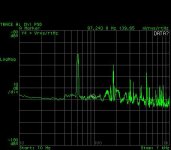
Noise increased about 40%. This is an important increase, but somehow less than expected. Does it make theoretical sense? Yes it does, though. It is enough to imagine the JFET with a source resistor as a new device, having an equivalent Vt' (that is, the algebraic sum of the original Vt and the voltage drop on the source resistor) and an equivalent Idss, that is the drain current at the new Vgs'=0 (that is, about 8mA). Now, for such a device, a strictly parabolic relationship between Id' and Vgs' doesn't really hold, unless Rs is very small (not the case here). However, we can get an image on what's happening; by adding a 360ohm resistor we added a significant noise source (has 2.4nV/rtHz). However, the noise gain is now 2*Vo/Vt' rather than 2*Vo/Vt and certainly Vt' is larger than Vt (again, because of the voltage drop on Rs). Therefore, adding a source resistor increases the equivalent device noise, but decreased the noise gain. From this tradeoff, the overall noise increases only 40% rather than in the ratio of device and equivalent device noises. The first picture below shows the noise spectra. As usual, the high imput impedance leads to some 60Hz pickup.
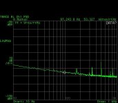
Now, (drums are rolling) the much expected case of a LED fed by a JFET. I used the same setup as above, but replaced the 2.2k resistor with the same red LED made in ACME China. The noise (in the second picture below) is marginally larger (less that 10%) and, if you consider that the current was increased to 8mA, could actually be thought as unchanged. This is again to be expected; after all, the JFET current source injects some noise by itself, as above, but the dynamic impedance of the LED is rather low. What is though remarkable is the effect of a combination of LED's rather low impedance with the good isolation with respect to the input voltage (due to the current source, rather than a simple resistor). The ratio between the LED dynamic impedance and the JFET output impedance is now very small, therefore the 60Hz pickup almost vanished.
And a last comment on LEDs. It is not unexpected that LEDs *may* have lower noise than any zener. After all, LEDS are forward biased junctions, and there's not much intrinsic sources (excluding second order effects) that would make a forward biased junction very noisy (as compared to impact ionization, etc... in breakdown junctions as zeners). Perhaps a forward biased diode is one of the best (from a noise perspective) reference device, but has only 0.6...0.7V. LEDs have more than that only because they are not build on silicon, but on a material with a much larger bandgap, otherwise, physically, they are, again, forward biased junctions. Now, there are good reason why I would not blindly trust LEDs as a low noise device; they are not designed for such, and the noise variations from manufacturer to manufacturer and batch to batch can be significant.
P.S. If I'll be in the mood over the weekend, I'll build such a buffer on a small board with SMD parts (I have some MMBFJ177 (J177 in SMD) from OnSemi) and then measure the Sij parameters up to 6GHz. That will end the myth of such a buffer having some amazing RF rejection properties. I did this before so I already know the answer The best rejections are for the LED and... for a simple resistive divider connected to the serial device base or gate (of course, decoupled to the ground).
Ok, so I took the best power supply buffer, the PN4392, measured here and added a gate-source resistor of 360ohm. Under the circumstances, the drain curent went down from 47mA (Idss) to about 8mA.
PN4392
-------
Datasheet:
Idss=25...75mA
Vt=2...5V
Vn@100Hz=Unspecified
Measured:
Rs=360ohm
R=2.2kOhm
Vo=17.8V
Noise=139.7nV/rtHz
Noise increased about 40%. This is an important increase, but somehow less than expected. Does it make theoretical sense? Yes it does, though. It is enough to imagine the JFET with a source resistor as a new device, having an equivalent Vt' (that is, the algebraic sum of the original Vt and the voltage drop on the source resistor) and an equivalent Idss, that is the drain current at the new Vgs'=0 (that is, about 8mA). Now, for such a device, a strictly parabolic relationship between Id' and Vgs' doesn't really hold, unless Rs is very small (not the case here). However, we can get an image on what's happening; by adding a 360ohm resistor we added a significant noise source (has 2.4nV/rtHz). However, the noise gain is now 2*Vo/Vt' rather than 2*Vo/Vt and certainly Vt' is larger than Vt (again, because of the voltage drop on Rs). Therefore, adding a source resistor increases the equivalent device noise, but decreased the noise gain. From this tradeoff, the overall noise increases only 40% rather than in the ratio of device and equivalent device noises. The first picture below shows the noise spectra. As usual, the high imput impedance leads to some 60Hz pickup.
Now, (drums are rolling) the much expected case of a LED fed by a JFET. I used the same setup as above, but replaced the 2.2k resistor with the same red LED made in ACME China. The noise (in the second picture below) is marginally larger (less that 10%) and, if you consider that the current was increased to 8mA, could actually be thought as unchanged. This is again to be expected; after all, the JFET current source injects some noise by itself, as above, but the dynamic impedance of the LED is rather low. What is though remarkable is the effect of a combination of LED's rather low impedance with the good isolation with respect to the input voltage (due to the current source, rather than a simple resistor). The ratio between the LED dynamic impedance and the JFET output impedance is now very small, therefore the 60Hz pickup almost vanished.
And a last comment on LEDs. It is not unexpected that LEDs *may* have lower noise than any zener. After all, LEDS are forward biased junctions, and there's not much intrinsic sources (excluding second order effects) that would make a forward biased junction very noisy (as compared to impact ionization, etc... in breakdown junctions as zeners). Perhaps a forward biased diode is one of the best (from a noise perspective) reference device, but has only 0.6...0.7V. LEDs have more than that only because they are not build on silicon, but on a material with a much larger bandgap, otherwise, physically, they are, again, forward biased junctions. Now, there are good reason why I would not blindly trust LEDs as a low noise device; they are not designed for such, and the noise variations from manufacturer to manufacturer and batch to batch can be significant.
P.S. If I'll be in the mood over the weekend, I'll build such a buffer on a small board with SMD parts (I have some MMBFJ177 (J177 in SMD) from OnSemi) and then measure the Sij parameters up to 6GHz. That will end the myth of such a buffer having some amazing RF rejection properties. I did this before so I already know the answer
The best rejections are for the LED and... for a simple resistive divider connected to the serial device base or gate (of course, decoupled to the ground).Attachments
Last edited:
This a very interesting discussion. I would tend to agree with Syn08's comments about the LM3xx not 'filtering'. These are active series regulators with a finite GBW, so they run out ouf steam quite quickly (approx 1 -2 MHz). However, in my view they are great devices that do a solid job.
For my part, I recently built an LM4562 op-amp based line pre-amp. I used simple 22 Ohm in series with each op-amp supply pin and then a high quality 100uF to ground (capacitor return paths are critical for noise in this approach). Since the LM4562 has outsranding PSSR, this is a valid approach. If you ar e designing discrete gain stages and/or using topologies with less PSSR (e.g. current feedback based), then you need something better in my view - series shunt arrangement.
For my part, I recently built an LM4562 op-amp based line pre-amp. I used simple 22 Ohm in series with each op-amp supply pin and then a high quality 100uF to ground (capacitor return paths are critical for noise in this approach). Since the LM4562 has outsranding PSSR, this is a valid approach. If you ar e designing discrete gain stages and/or using topologies with less PSSR (e.g. current feedback based), then you need something better in my view - series shunt arrangement.
"I have had good results placing a simple RC filter before the 317/337. It helps roll off the RFI before it reaches the first transistor in the regs. Perhaps we could insert another RC after the 317/337 to filter before the 2nd reg."
Another approach is to do this on the primary side of the transformer.
Another approach is to do this on the primary side of the transformer.
"I have had good results placing a simple RC filter before the 317/337. It helps roll off the RFI before it reaches the first transistor in the regs.
I now that inductors are evil around these parts from the audiophile perspective, but is anyone here aware of just how effective a little LC RF filtering on the input side of the regulator can be??????????
I'm not talking 10H chokes here.
You changed the load resistor (Rl) and that is why you got more noise. Noise (total) is related to Gm Rl, low Rl, low noise.
Nope. Changing only the resistor Rl would lead to a contribution of SQRT(2.4k/0.36k)=2.6 times more noise, or 260%. This is not the case.
Obviously, you forgot what you read a couple of days ago. Read again about the noise gain in this configuration: http://www.diyaudio.com/forums/soli...rch-preamplifier-part-ii-200.html#post1963702
PMA, thanks, once again, for your input. I might say that Jan asked a proper question, just because it is true the higher frequency gives higher self noise on a scope. We all agree to that. However, you are referring to a lot of RF from the power line getting through, I suspect, and you are right. Sometimes we have to let others come to that conclusion, before it will 'stick' and later be obvious in future to 'everyone'. Keep up the good work, PMA
PMA, thanks, once again, for your input. I might say that Jan asked a proper question, just because it is true the higher frequency gives higher self noise on a scope. We all agree to that. However, you are referring to a lot of RF from the power line getting through, I suspect, and you are right. Sometimes we have to let others come to that conclusion, before it will 'stick' and later be obvious in future to 'everyone'. Keep up the good work, PMA


Gm Rl does not have any square root in it, so far as I can see.
Then the noise should be x6 larger, which is not. Really John, I know it's hard for you, but you need to go back and read.
With Jfet will do better.It will at least skip some of the 60Hz.
The ratio between the LED dynamic impedance and the JFET output impedance is now very small, therefore the 60Hz pickup almost vanished.
Thanks for confirming syn. After all if you think about it, its simplistic.
On a more serious note, cheers for the experiments. Very interesting for all of us with just 20MHz scopes and a DVM.
P.S. Thanks to you noisebusters (especially syn08 and anatech) I am confident about my low MC input stage to be made. Its nice when practical things are born. I will use 2N5459 which is dirt cheap, available, and has some Vt. With Idss at about 5mA bunch up in my zip bag, the leds are going to work enough too.
Attachments
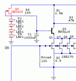
Ok, so I took the best power supply buffer, the PN4392, measured here and added a gate-source resistor of 360ohm. Under the circumstances, the drain curent went down from 47mA (Idss) to about 8mA.
PN4392
-------
Datasheet:
Idss=25...75mA
Vt=2...5V
Vn@100Hz=Unspecified
Measured:
Rs=360ohm
R=2.2kOhm
Vo=17.8V
Noise=139.7nV/rtHz
Noise increased about 40%. This is an important increase, but somehow less than expected. Does it make theoretical sense? Yes it does, though.
It doesn't make sense to me. These are the specs I found for the PN4392:
gfs = 6mS
gos = 25uS
en = 3nV/rtHz
Theory says that if a resistor Rs is connected between G and S pins then the output conductance of the circuit is
go = gos^2 / (1 + Rs * (gos + gfs))
then for the PN4392 and the values above
go = (0.000025)^2 / (1 + 360 * (0.000025 + 0.006))
so
go = 0.197nS
The voltage gain should be
Av = go * R
or
Av = 0.197nS * 2200 = 0.434u
The noise should be the sqrt of the sum of the square of the noise of the 2200 resistor and of the jfet+Rs device.
The noise of the 2200 at 22C is about 6nV/rtHz, let's call this enR.
The noise of the 360 resistor at 22C is about 2.4nV/rtHz, let's call this enRs
The noise of the PN4392 is 3nV/rtHz, let's call this enj
So the noise of the jfet+Rs should be
sqrt(enRs^2 + enj^2) = 3.842nV/rtHz
and we multiply this by the gain Av and get
0.000000434 * 0.000000003842 * 2200 = 3.67 * 10^-12 nV/rtHz
You get the point. This should get added to 6nV/rtHz, the noise of the 2200 resistor, but let's not bother. From this analysis the noise of the resistor dominates.
How can this make sense? Can anyone spot the mistake?
It doesn't make sense to me. These are the specs I found for the PN4392:
gfs = 6mS
gos = 25uS
en = 3nV/rtHz
Theory says that if a resistor Rs is connected between G and S pins then the output conductance of the circuit is
go = gos^2 / (1 + Rs * (gos + gfs))
Can anyone spot the mistake?
Not sure where you got these formulas from, but something stinks. Left side is dimensionally a conductance, right side is a squared conductance.
Not sure where you got these formulas from, but something stinks. Left side is dimensionally a conductance, right side is a squared conductance.
From the book I mentioned before, "Current sources and voltage references" by Linden T. Harrison
I think I know where I went wrong. I used the dynamic output conductance in the gain calculation instead of the transfer conductance. In essence, just like making the mistake of using gos instead of gfs for the case of G and S tied together.
Attachments
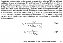
Not sure where you got these formulas from, but something stinks. Left side is dimensionally a conductance, right side is a squared conductance.
.. but isn't the right side a squared conductance over a conductance = conductance, dimensionally?
jd
Now this makes more sense. The way I see it (and for you guys this has been clear all along) is that using the G-S resistor decreases the gain of the circuit, hence decreases the multiplier in the noise calculation. In the same time there is more resistance in the circuit, which increases the noise. Obviously there is a sweet point where the gain multiplier and the added resistor noise is lowest.
For the PN4392 you tested,
Idss = 47mA
Ids = 8mA
en = 3nV/rtHz
Rs = 360 ohm
R = 2200 ohm
Vt = 4V
First let's calculate
gfs = 2 * Idss / Vt
= 2 * 0.047 / 4
= 23.5mS
The circuit transfer conductance, gfs prime:
gfs' = 2 * sqrt( Idss * Id) / Vt
= 2 * sqrt(0.047 * 0.008)/4
= 9.695 mS
At Idss, when Vgs = Vt, the resistor to set the reference voltage Vo is smaller than when Rs is used between G and S, but gfs = 23.5mS is higher.
Doing the same substitutions as syn08 did to get the gain
Au = gfs * R = 2*Vo/Vt
we get
Au' = 2 * sqrt (Idss * Vo * R / Vt^2)
which still shows the large role of Vt, the pinch-off voltage.
.. but isn't the right side a squared conductance over a conductance = conductance, dimensionally?
jd
It is not. The 1 + R*g denominator is adimensional. The second eq. is dimensionally correct, but I think it's valid only in special circumstances, like small Rs. I don't know and I don't have that book.
Now this makes more sense. The way I see it (and for you guys this has been clear all along) is that using the G-S resistor decreases the gain of the circuit, hence decreases the multiplier in the noise calculation. In the same time there is more resistance in the circuit, which increases the noise. Obviously there is a sweet point where the gain multiplier and the added resistor noise is lowest.
For the PN4392 you tested,
Idss = 47mA
Ids = 8mA
en = 3nV/rtHz
Rs = 360 ohm
R = 2200 ohm
Vt = 4V
First let's calculate
gfs = 2 * Idss / Vt
= 2 * 0.047 / 4
= 23.5mS
The circuit transfer conductance, gfs prime:
gfs' = 2 * sqrt( Idss * Id) / Vt
= 2 * sqrt(0.047 * 0.008)/4
= 9.695 mS
At Idss, when Vgs = Vt, the resistor to set the reference voltage Vo is smaller than when Rs is used between G and S, but gfs = 23.5mS is higher.
Doing the same substitutions as syn08 did to get the gain
Au = gfs * R = 2*Vo/Vt
we get
Au' = 2 * sqrt (Idss * Vo * R / Vt^2)
which still shows the large role of Vt, the pinch-off voltage.
I think you got it right this time. You may want to explain this to JC, apparently I failed miserably.
I still think there's a typo in the book, or they use some normalized variables, otherwise still something is wrong.
- Status
- Not open for further replies.
- Home
- Member Areas
- The Lounge
- John Curl's Blowtorch preamplifier part II