That graph, in NO WAY looks like the graph in Buckingham's book.
From your statements, that's quite certain. So I'm not exactly sure what you are talking about. Their test results appear to be quite smooth and continuous.
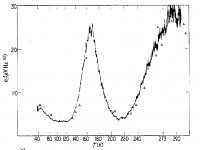
They show a minima at about 210K, a peak at about 165K, another dip at 110K, seemingly consistent with your verbage. But H and K's graph of the individual frequencies vs temperature I posted previously doesn't match your verbage with respect to weird behaviour..so I certainly have to question the odd hypothesizings you provided.
Did Buckingham massage data from two sources?
Can you produce the graph you speak of?
jn
Attachments
Last edited:
Buckingham does discuss WHY there are the differences in this graph in his book.
Well??
jn
Well, what? Please, either get a copy of Buckingham's 'Noise in Electronic Devices and Systems' from your company library, and look at go to p.130 and look at the graph itself.
OR get the paper it is referenced from. Then you compare.
You should have better access to the IEEE archives through your company so that it doesn't cost you anything.
I am NOT the author here, I am just citing references.
OR get the paper it is referenced from. Then you compare.
You should have better access to the IEEE archives through your company so that it doesn't cost you anything.
I am NOT the author here, I am just citing references.
ps... I've also used this technique for computer controlled ultrasonic welder where I needed to know exactly how much power was being dissipated by the load. The ultrasonic transducer/horn assembly has an unloaded Q of roughly 10,000, so requires extreme control of drive. A simple .1 ohm resistor for current monitoring caused excessive phase shift of the measured voltage, which resulted in an incorrect measure of power delivered vs power reflected. So I used 3 pieces of 300 milliohm resistors in parallel, tightly packed body to body, and ran the v tap wire up the physical center between the 3 cylinders. Worked perfectly.
Cheers, Jn
This is a large part of why I proposed the use of multiple fuses in parallel for an amplifier's AC connectivity, rather than the one fuse. The sonic advantages are as obvious as can be regarding the development of complex harmonic structures in the final sonic presentation ...as they were (regarding base functionality) with your application. The fuses, like your application, are going to need to be from the same batch, design, build, etc..if it is going to be workable.
Ran outta editing time..
JC..
I certainly have to question the odd hypothesizings you provided. These statements...""This is where reality defies engineering approximation "", and ""It is like the excess noise on whatever device they used is composed of a series of wobbles, perhaps quantum related, and no smooth curve."" are certainly not supported by H and K's graphs..
That's why I asked about what exactly Buckingham was using for data. Using two independent and uncorrelated sources spliced into one graph could certainly do weird things to a graph...
From the looks of H and K's data, there doesn't appear to be anything weird happening. Just the normal carrier recombination funnies that happen in a cryo environment.. I've had my share of those, Vf at 4.5 Kelvin running 3 to 30 volts, now that's weird..
jn
This is a large part of why I proposed the use of multiple fuses in parallel for an amplifier's AC connectivity, rather than the one fuse. The sonic advantages are as obvious as can be regarding the development of complex harmonic structures in the final sonic presentation ...as they were (regarding base functionality) with your application. The fuses, like your application, are going to need to be from the same batch, design, build, etc..if it is going to be workable.
Multiple fuses in that application have nothing to do with what you copied of my work.
I used the null location of the current centroid to place a tap wire for measurement of the resistance without creating a loop for trapping of time varying flux, that flux causing out of phase voltage by induction. And all the induced voltage was the primary frequency, not any harmonics. Multiple fuses has nothing to do with the terminal voltages present across the fuses, other than a simple reduction in resistance that could be had by using a larger fuse.
jn
If I didn't explain myself fully, John, that does not mean that I'm wrong. It merely means that there is room for misinterpretation. And when you and I address one another, that is the road it goes down, most times. I understand that your job and work requires specifics and potentials to be fully addressed, but mine does not. One might consider that you are in that life and place as this is complementary to how you are wired.
I can accept that differential.
My capacity to wander is what takes me into different areas, questions, answers and solutions. It does not mean that I'm wrong, but that the back and forth probably does not satisfy your I/O system.
")
I do not understand your "not smooth" comments. The graphs in Haslett and Kendall are quite smooth and continuous.
What exactly did Buckingham print??
jn
This is the classic generation-recombination noise behavior, if you want I can post dozens of plots from many vendors. It is not per se 1/f noise but a special case of a dominant type of recombination center with a time constant that has an activation energy. You can literally change some devices 10 degrees and get 100X the noise. It's spectrum is Lorentzian with a time domain apperance of a random telegraph signal.
From the looks of H and K's data, there doesn't appear to be anything weird happening. Just the normal carrier recombination funnies that happen in a cryo environment.. I've had my share of those, Vf at 4.5 Kelvin running 3 to 30 volts, now that's weird..
jn
Thru what materials, John, if you would be so kind?
Did Buckingham massage data from two sources?
Can you produce the graph you speak of?
jn
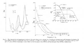
I have dozens of these plots too, it does not always require cryo temperatures. I just checked Buckingham and his plot is spot frequencies with a temperature sweep taken from H&K. Mine are .1-10Hz noise with a slow temperature sweep, different ways of looking at the same thing. BTW I posted a plot in the Pass forum of a beloved 2SK170 with GR noise. These contaminations and defects are something that folks try to eliminate and we have been getting better at it, there are many JFET's with little or none of this.
Last edited:
Looking at graphs in the 'Siliconix FET design catalog' July 1983 of various Nchannel jfets that I have used over the decades, most are 'smoothed' graphs, some are somewhat irregular, which says that something is going on that is not smooth, and my own Quantech measurements have shown this problem with different devices and geometries.
However, H&K's graph on p. 130, of Buckingham's book is spectacular, and was put there to be so, in order to show the mechanisms that can make excess noise greater in some devices, and at some temperatures, that some predicted average. Still, it appears to be a real and direct measurement of an Nch jfet considered 'low noise' at the time. This is stated in the text.
Please look up the references for further clarification.
'proof' is a nice thing to encounter, if one feels that such is necessary. Proofs come after after observation, after hypothesis, after testing, after fact and after reality, not before.
Kinda obvious, but some folks tend to get confused, regarding the OOO way out at the edge of things. Carts and horses and all that.
Still, this should help some.
Making superconducting nanocircuits with rounded corners will improve their performance, according to John R. Clem, a physicist at the U.S. Department of Energy’s Ames Laboratory, and Karl K. Berggren, an associate professor of electrical engineering at the Massachusetts Institute of Technology.
Cutting corners to make superconductors work better
Something that good audio designers have known for a very long time.
Last edited:
Ken I'm surprised to see you quote ordinary good science and engineering.
Who is designing audio equipment with superconducting nanocircuits? Not many, possibly nobody? The cited work appears to be about current crowding at corners, so the current density gets too high. Important for superconductors in nanocircuits, completely irrelevant for good conductors in ordinary PCBs?KBK said:Something that good audio designers have known for a very long time.
I understand you are not the author. And it was nice of you to reference H and K, the source of Buckingham's data so that I could aquire H and K's paper to read.Well, what? Please, either get a copy of Buckingham's 'Noise in Electronic Devices and Systems' from your company library, and look at go to p.130 and look at the graph itself.
OR get the paper it is referenced from. Then you compare.
You should have better access to the IEEE archives through your company so that it doesn't cost you anything.
I am NOT the author here, I am just citing references.
So I actually did go to the source of the information, only to find the normal nice graphs expected, not some weird discontinuity thingy. That is why your statements were confusing, as they were inconsistent with the base data being referred to.
If I didn't explain myself fully, John, that does not mean that I'm wrong. It merely means that there is room for misinterpretation. And when you and I address one another, that is the road it goes down, most times. I understand that your job and work requires specifics and potentials to be fully addressed, but mine does not. One might consider that you are in that life and place as this is complementary to how you are wired.
I can accept that differential.
My capacity to wander is what takes me into different areas, questions, answers and solutions. It does not mean that I'm wrong, but that the back and forth probably does not satisfy your I/O system.
You are incorrect in the bulk of what you just stated. The capacity to wander is not something to be ridiculed, and I have not done so. My "I/O system" is in no way "unsatisfied" by your statements. I simply pointed out that the physics I described using, to fix as specific problem, was inconsistent in application to fuses. I used the geometry to remove the inductance from the measurement of a time varying current. I needed to do so to eliminate the phase shift of the magnetic field of the resistor for the instantaneous calcuation of delivered power to the load.
As such, the physics I specified have nothing to do with the changing of the external field of the current path, but rather, a way to get around that field to accurately measure the drop across the resistor. It is not a method of getting around any non-linearity.
Thru what materials, John, if you would be so kind?
A normal silicon diode. It turns out that at 4.5 kelvin, my diodes do not conduct current until the forward voltage exceeds a rather large threshold. My diodes were specified to remain non conducting at a minimum of 3 volts and a maximum of 8 volts. Once conduction was started, the die heated up sufficiently that the diode then switched back to normal diode conduction behaviour. Kind of like an SCR or crowbar circuit. The diodes reacted quite fast, as there is virtually no heat capacity in silicon or copper at 4.5 kelvin. Only the helium has capacity there. The diode and copper sinks (16 cubic inches of copper) climb to 50 kelvin very rapidly, where heat capacity returns.
MRI's typically require thresholds in the 30 volt range. The big guys, like powerex, know very well how to diffuse these puppies to get the threshold they need. Me, I just spec what I need, they make em...
Who is designing audio equipment with superconducting nanocircuits? Not many, possibly nobody? The cited work appears to be about current crowding at corners, so the current density gets too high. Important for superconductors in nanocircuits, completely irrelevant for good conductors in ordinary PCBs?
Actually, on silicon it can be rather important. Electromigration will occur in aluminum at current densities near 10 power 6 amps per ccm squared (If I recall accurately), this was a problem as transistors became smaller.. Nowadays, they know better. But you are correct, on PCB's, it is not possible to get those current densities, as the g-10 is incapable of sufficient heat transfer to keep the copper under about a thousand degrees C...
Cold, the guys at CERN have to worry about this as well, as the tin/silver solder joints (like the one that exploded) can achieve 10 power 5 amps per cm squared in the solder, and that will push those atoms to one side of the joint through repeated quenches..not good...
I can see how corners with supers would be a problem. If the current tries to exceed Jc at a corner, it'll quench...but that's also standard RF stuff as well.
Cheers, jn
Last edited:
Jneutron, the graph put into Buckingham's book was chosen to show problems with temperature in predicting 1/f noise. If your Brookhaven library does not have a copy, will why not rely on Scott's input? IF you have a fax, I might even send you a copy of the graph that I cited. It looks like the Alps, not any gentle slope.
Why you quibble with me on THIS thread, when low noise jfet electronics is continually cited here, is beyond my understanding.
Why you quibble with me on THIS thread, when low noise jfet electronics is continually cited here, is beyond my understanding.
Here is one of their plots with several ways of looking at it. Buckingham's plot is like the one on the left. This stuff has been worked on since 1964 (Sah) gold is not a contaminant of importance anymore, it's known as learning how to do stuff right. Note the 300K plot on right, just like a recent 2SK170.
Attachments
Last edited:
- Status
- Not open for further replies.
- Home
- Member Areas
- The Lounge
- John Curl's Blowtorch preamplifier part II