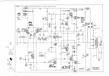
JLH Powertran as modified by Radio Spares & TV in 1975
Thanks for putting up with my questions as I get the hang of this site.
Apologies if this should be a post on its own, but if you look at the circuit that I have uploaded that I built my amp from, apart from a few changes in resitor values and new transistors, the layout is an (almost) identical copy.
I will appreciate members comments on updating the transistors to ones more easily obtained in 2014, as I am having a deil of a job getting valid substitutes - perhaps as a result of shop assistants seeing a 70+ yo granny asking for these things !!!!
In the rebuild below, I fried my output transistors yesterday. Any ideas why, and what I should check for (no shorts between tracks, pins in correct slots as far as I know). I am on the verge of giving up!
Thanks
Joy Wellbeloved
Tr #
IN blown AMP 2014
1/7/14 rebuild
IN POWERTRAN
1
MPSA55 EBC
MPSA56 EBC
BFR79
2
2N3819 DGS
2N3819 DGS
2N5459
3
NSDU06 EBC
OLD NSDU06
BFR39
4
BC212 EBC
OLD BC212
BFR79
5
BF259 CBE
BF259 CBE
BF258
6
BC108 EBC
BC108 EBC
BC184
7
BC167 ECB
OLD BC167
BC182
8
BC257 ECB
BC257A ECB
BC212
9
TIP30C BCE
BD240C BCE
BD530
10
TIP29C BCE
BD239C BCE
BD529
11
2N3055 BEC
2N3442 BEC
BDY56
12
2N3055 BEC
2N3442 BEC
BDY56
Attachments
As this amplifier once worked, and if no signs of overheating, I can't imagine much would have changed over time apart from physical damage and the electrolytic capacitors drying out and failing - perhaps frying a few semis in the process of powering it up in that condition.
Many of the substitutes are just not up to original spec but at only +/- 33V power supply, most should work if their orientation and pin array is compatible with the PCB. This sometimes isn't the case. I can say right now that MPSA parts are different pinout to original but you have that covered, I see. To check, you can simply search "ABC 123 pinout" with Google and bingo! - answers. Also likely are the diodes if the cathode marking or band marked end is not correct. Assuming the PCB predates a printed overlay to guide you, you could have errors with D1, ZD1 too.
Normal test procedure for dead amplifiers is to build a bulb limiter to restrict current and damage to that which can flows through an incandescent lightbulb: http://www.diyaudio.com/forums/equipment-tools/252386-bulb-limiter-testing.html
This at least will allow you to test voltages as necessary to verify if parts are working correctly and showing the proper voltage from Base to Emitter of ~ 0.65V, +or- , depending on N or P type.
Take a look at the schematics I linked to earier showing you substitutes others have already used. That should help with some components but unless you have means of testing, checking operation, it may not be the way to go by simply replacing everything, only to see it fail again.
Perseverance
Many thanks Ian.
So far - I have removed the PCB from the chassis, and removed every componenet from it. Cleaned up the tracks, opening all lead holes. I then replaced all the resistors, caps and diodes, checking a photo taken before stripping to ensure all correct.
I have googled and found various sites to give me the pin layouts, and have checked those to the pcb to determine which leg goes where. Finally I inserted the transistors and did a first test. Idling current was way too high, and output transistors got very hot - with one blowing.
I think my next steps are to remove all transistors, test them, and replace once again with good ones and test again. Actual line voltage is 45+ and -.
Any other input will be greatly appreciated ! (Thanks to the wonders of the internet!)")
Joy
Many thanks Ian.
So far - I have removed the PCB from the chassis, and removed every componenet from it. Cleaned up the tracks, opening all lead holes. I then replaced all the resistors, caps and diodes, checking a photo taken before stripping to ensure all correct.
I have googled and found various sites to give me the pin layouts, and have checked those to the pcb to determine which leg goes where. Finally I inserted the transistors and did a first test. Idling current was way too high, and output transistors got very hot - with one blowing.
I think my next steps are to remove all transistors, test them, and replace once again with good ones and test again. Actual line voltage is 45+ and -.
Any other input will be greatly appreciated ! (Thanks to the wonders of the internet!)
Joy
Really, +/- 45V is too high for 2N3055 transistors. They may survive the set up process but life will be short for them when you play music at decent levels through them.
If possible, use On-Semi MJ15003 for the output transistors and TIP42 for TR9, TIP41 for TR10. All are relatively cheap and widely available parts for the output stage. They will take quite some abuse but with a bulb limiter/tester you should not need further protection for getting it going.
As you describe what occurred, it seems to me as if you powered up with the bias current setting full on and this will cause thermal runaway, overheating and failure of the output transistors - possibly the driver transitors too, in short order. You need to pre-set the movable contact on the bias potentiometer (2.2k) at the minimum bias position - closest to TR6 base connection before powering up. This should minimise bias which you can later increase to the correct setting, when all else is working correctly.
Note that the bias current is measured as so many mV drop across either large 0.22-0.33 ohm resistor in the output stage. It seems the original 0.27 value was hard to find.
- Status
- This old topic is closed. If you want to reopen this topic, contact a moderator using the "Report Post" button.